Zynq-7000 AP SoC and 7 Series FPGAs MIS v4.1 269
UG586 November 30, 2016
www.xilinx.com
Chapter 1: DDR3 and DDR2 SDRAM Memory Interface Solution
vio_fixed_instr_value = 1 (Read Only)
vio_pause_traffic = 0
5. Observe the dbg_rddata_r and cmp_data_r signals in Vivado logic analyzer feature.
This can also be done using high quality probes and a scope using the Traffic Generator or
your own user design.
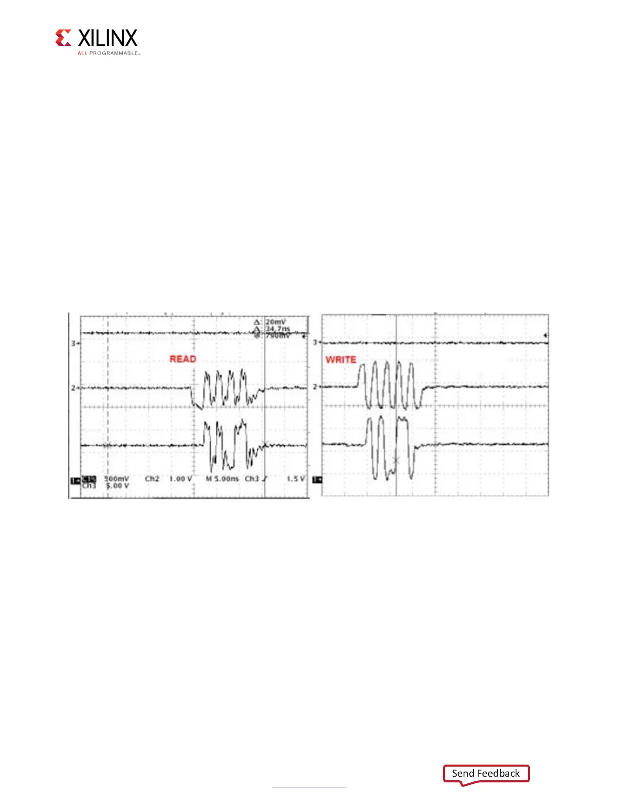
1. Capture the write at the memory and the read at the FPGA to view data accuracy,
appropriate DQS-to-DQ.
2. Look at the initial transition on DQS from 3-state to active.
3. During Write, DQS does not have a preamble.
4. During Read, the DQS has a Low preamble that is 1 clock cycle long.
5. The following is an example of a Read and a Write to illustrate the difference.
Analyze write timing:
• If on-die termination (ODT) is used, check that the correct value is enabled in the
DDR2/DDR3 device and that the timing on the ODT signal relative to the write burst is
correct.
• Measure the phase of DQ relative to DQS. During a Write, DQS should be center aligned
to DQ. If the alignment is not correct, focus on the debugging OCLKDELAYED
Calibration, page 150.
• For debugging purposes only, use ODELAY to vary the phase of DQ relative to DQS.
Analyze read timing:
X-Ref Target - Figure 1-106
Figure 1-106: Read and Write
 Loading...


