Zynq-7000 AP SoC and 7 Series FPGAs MIS v4.1 445
UG586 November 30, 2016
www.xilinx.com
Chapter 3: RLDRAM II and RLDRAM 3 Memory Interface Solutions
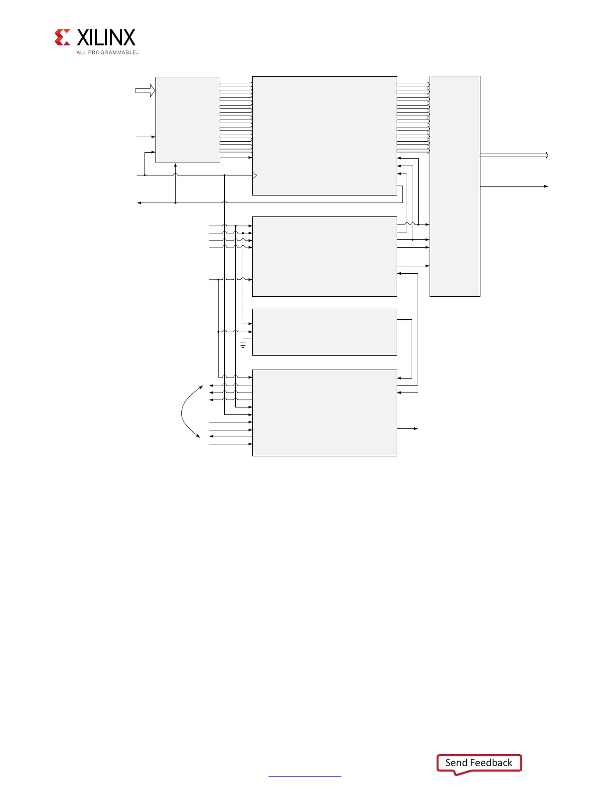
The OSERDES blocks available in every I/O simplifies generation of the proper clock,
address, data, and control signaling for communication with the memory device. The flow
through the OSERDES uses two different input clocks to achieve the required functionality.
Data input ports D1/D2 or D3/D4 are clocked in using the clock provided on the CLKDIV
input port, and then passed through a parallel-to-serial conversion block. The OSERDES is
used to clock all outputs from the PHY to the memory device. Upon exiting the OSERDES, all
output signals must be presented center-aligned with respect to the generated clocks
(CK/CK# for address/control signals, DK/DK# for data and data mask). For this reason, the
PHASER_OUT_PHY block is also used in conjunction with the OSERDES to achieve center
alignment.
X-Ref Target - Figure 3-50
Figure 3-50: Write Path Block Diagram of the RLDRAM II Interface Solution
Output data to a byte group
Write_enable from FPGA logic
Of_full
Phy_clk
OLOGIC
(OSERDES/
ODDR)
PRE_FIFO
D
WREN
CLK
Q
OUT_FIFO
D0[3:0]
D1[3:0]
D2[3:0]
D3[3:0]
D4[3:0]
D5[7:0]
D6[7:0]
D7[3:0]
D8[3:0]
D9[3:0]
WRCLK
WREN
Q0[3:0]
Q1[3:0]
Q2[3:0]
Q3[3:0]
Q4[3:0]
Q5[7:0]
Q6[7:0]
Q7[3:0]
Q8[3:0]
Q9[3:0]
RST
RDCLK
RDEN
FULL
FRE
QBB
PHASER_OUT_PHY
MEMREFCLK
FREQREFCLK
FINEENABLE
FINEINC
RST
OSERDESRST
RDENABLE
OCLKDIV
OCLK
OCLKDELAYED
BURSTPENDINGPHY
PHASER_REF
CLKIN
RST
PWRDWN
LOCKED
PHY_CONTROL
RESET
PHYCTLALMOSTFULL
PHYCTLFULL
PHYCTLREADY
MEMREFCLK
PHYCLK
PHYCTLWD
PHYCTLWRENABLE
PLLLOCK
SYNCIN
REFDLLLOCK
OUTBURSTPENDING
PHYCTLMSTREMPTY
PHYCTLEMPTY
OSERDES O/P to memory
(rldii_dq, rldii_dm)
Write clocks to memory
(rldii_dk/rldii_dk#)
From Master phy_control
To other phy_control blocks
From PLL
Of_rd_en
From PLL
From PLL
From Initialization Logic
From Initialization Logic
rst
To/From Initialization Logic
 Loading...


