Zynq-7000 AP SoC and 7 Series FPGAs MIS v4.1 535
UG586 November 30, 2016
www.xilinx.com
Chapter 4: LPDDR2 SDRAM Memory Interface Solution
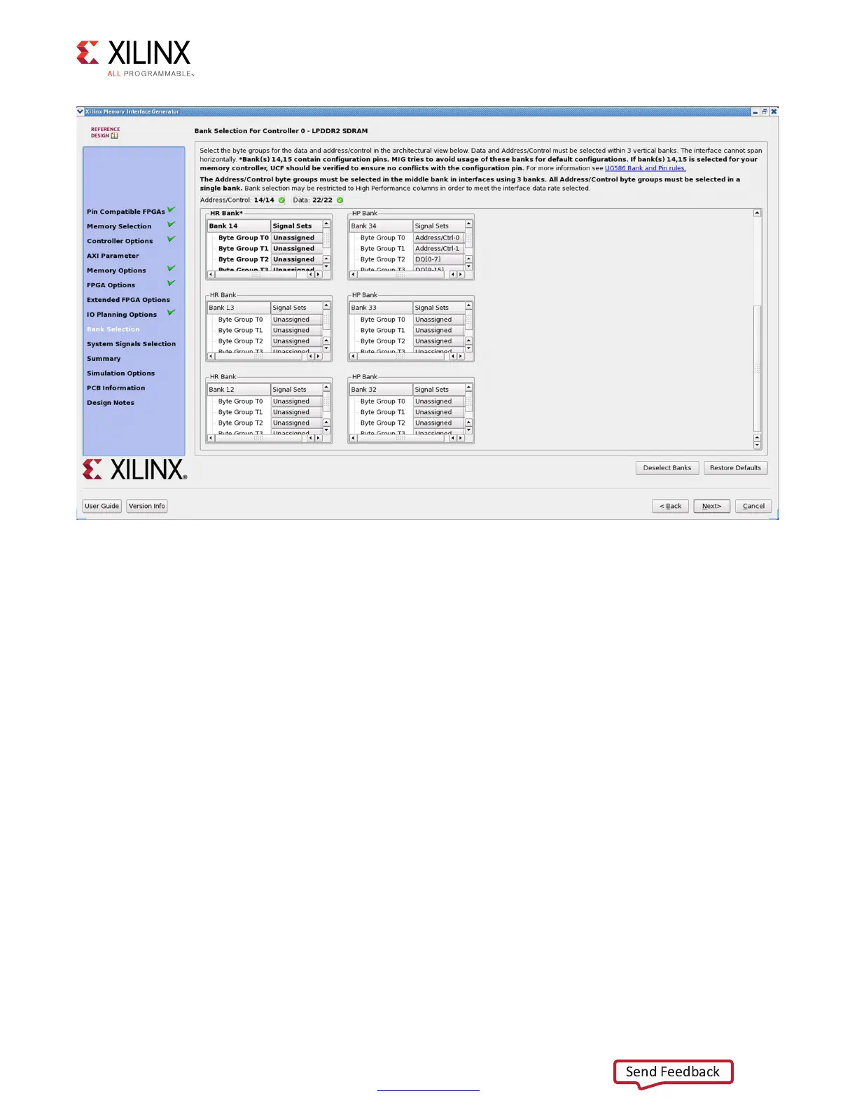
For customized settings, click Deselect Banks and select the appropriate bank and memory
signals. Click Next to move to the next page if the default setting is used.
To unselect the banks that are selected, click Deselect Banks. To restore the defaults, click
Restore Defaults.
VCCAUX_IO groups are shown for HP banks in devices with these groups using dashed lines.
VCCAUX_IO is common to all banks in these groups. The memory interface must have the
same VCCAUX_IO for all banks used in the interface. MIG automatically sets the VCCAUX_IO
constraint appropriately for the data rate requested.
For devices implemented with SSI technology, the SLRs are indicated by a number in the
header in each bank, for example, SLR 1. Interfaces cannot span across Super Logic Regions.
Select the pins for the system signals on this page (Figure 4-24). The MIG tool allows the
selection of either external pins or internal connections, as desired.
X-Ref Target - Figure 4-23
Figure 4-23: Bank Selection
 Loading...


