Reference Manual ADuCM356
HIGH-SPEED DAC CIRCUITS
analog.com Rev. A | 107 of 312
Gain calibration is optional and adjusts the peak-to-peak voltage
swing. The peak-to-peak voltage swing can also be adjusted by
changing the minimum and maximum DAC codes.
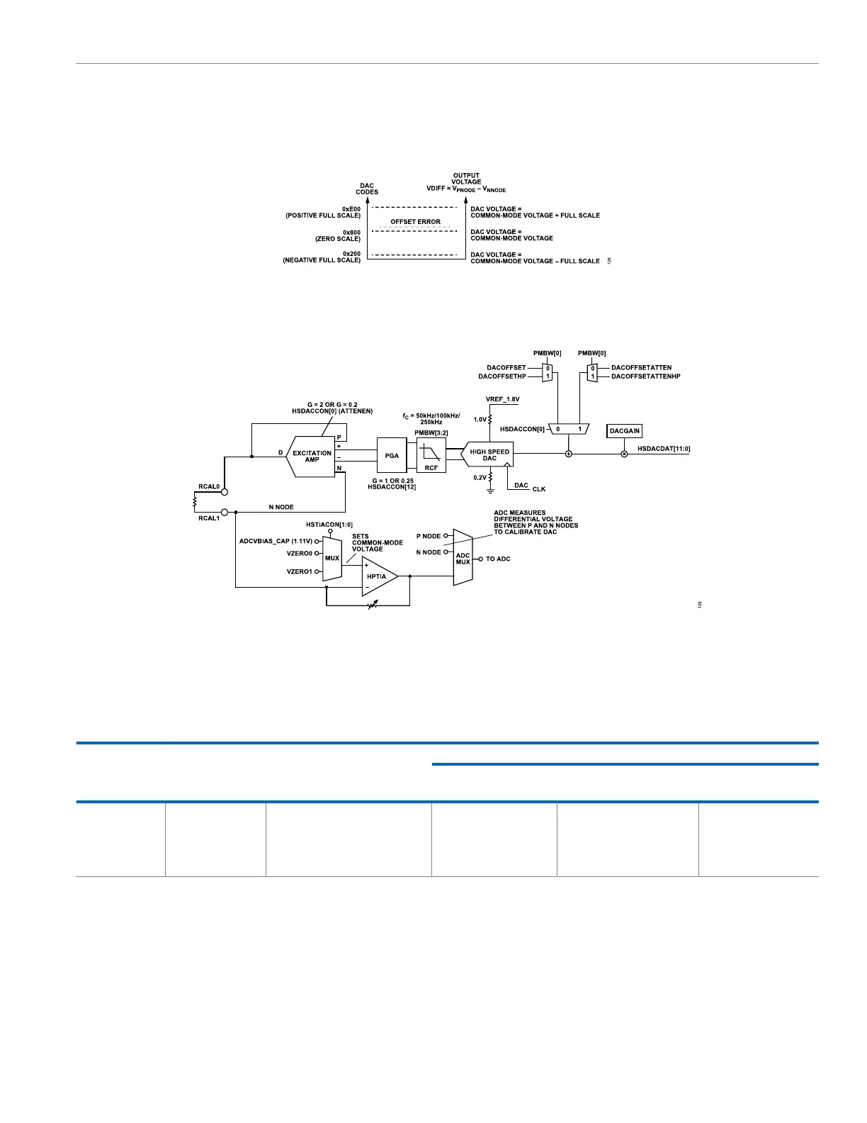
Figure 25. High-Speed DAC Transfer Function
The high-speed DAC transfer function is shown in Figure 25.
Note that in Figure 26 the common-mode voltage setting for the
calibration circuit is set by the noninverting input of the high speed
TIA.
Figure 26. High-Speed DAC Calibration Circuit Using R
CAL
The example functions provided in the EVAL-ADuCM356QSPZ kit
demonstrate how to use the ADC to measure the differential voltage
across R
CAL
and how to adjust the appropriate offset calibration
resistor until this differential voltage is approximately 0 V.
Table 127 shows the appropriate calibration for each high-speed
DAC output setting and the selected power mode of the analog die.
Table 127. High-Speed Calibration Register Assignment for Each Output Range
HSDACCON,
Bit 12 Setting
HSDACCON,
Bit 0 Setting
Typical Output Range
(Code 0x200 to Code 0xE00)
Relevant Calibration Registers
Low-Power Mode High-Power Mode
Low-Power Mode/
High-Power Mode
0 0 ±607 mV DACOFFSET DACOFFSETHP DACGAIN
1 0 ±75 mV DACOFFSET DACOFFSETHP DACGAIN
1 1 ±15.14 mV DACOFFSETATTEN DACOFFSETATTENHP DACGAIN
0 1 ±121.2 mV DACOFFSETATTEN DACOFFSETATTENHP DACGAIN
 Loading...