EasyManua.ls Logo

Analog Devices ADuCM356 User Manual

Analog Devices ADuCM356
312 pages
To Next Page IconTo Next Page
To Previous Page IconTo Previous Page
Page #239 background imageLoading...
Page #239 background image
Reference Manual ADuCM356
SERIAL PERIPHERAL INTERFACES
analog.com Rev. A | 239 of 312
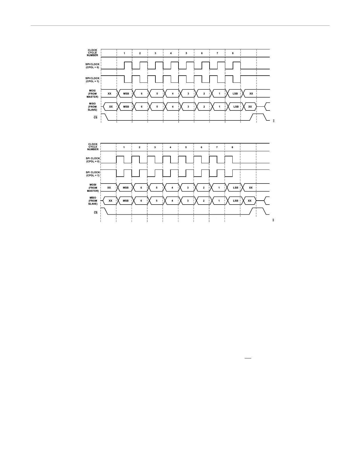
Figure 61. SPI Transfer Protocol, CPHA = 0
Figure 62. SPI Transfer Protocol, CPHA = 1
Transfers in Target Mode
In target mode, a transfer is initiated by the assertion of the chip
select of the device. Though the initiator can support up to four
chip select output lines, only one chip select input is used in target
mode. The device as a target transmits and receives 8-bit data until
the transfer is concluded by the deassertion of chip select. The SPI
transfer protocol diagrams in Figure 61 and Figure 62 illustrate the
data transfer protocol for the SPI, and the effects of SPIx_CTL, Bit
2 and SPIx_CTL, Bit 3 on that protocol. The chip select must not be
tied to the ground.
SPI Data Underrun and Overflow
If the transmit zeros enable bit (SPIx_CTL, Bit 7) is cleared, the last
byte from the previous transmission is shifted out when a transfer is
initiated with no valid data in the FIFO. If SPIx_CTL, Bit 7 is set to
1, 0s are transmitted when a transfer is initiated with no valid data
in the FIFO. If the receive overflow overwrite enable bit (SPIx_CTL,
Bit 8) is set, and there is no space left in the FIFO, the valid data
in the receive FIFO is overwritten by the new serial byte received. If
SPIx_CTL, Bit 8 is cleared, and there is no space left in the FIFO,
the new serial byte received is discarded. When SPIx_CTL, Bit 8
is set, the contents of the SPI receive FIFO are undefined, and its
contents must be discarded by user code.
Full Duplex Operation
Simultaneous reads and writes are supported on the SPI. When im-
plementing full duplex transfers in initiator mode, use the following
procedure:
1. Initiate a transfer sequence via a transmit on the P0.1/
SPI0_MOSI pin and the P1.3/SPI1_MOSI pin. Set SPIx_CTL,
Bit 6 = 1. If interrupts are enabled, interrupts are triggered when
a transmit interrupt occurs but not when a byte is received.
2. If using interrupts, the SPI transmit interrupt indicated by
SPIx_STAT, Bit 5 or the transmit FIFO underrun interrupt
(SPIx_STAT, Bit 4) is asserted approximately three to four SPI
clock periods into the transfer of the first byte. If necessary,
reload a byte into the transmit FIFO by writing to the SPIx_TX
register.
3. The first byte received via the MISO pin does not update the
receive FIFO status bits (SPIx_FIFO_STAT, Bits[11:8]) until 12
SPI clock periods after CS goes low. Therefore, two transmit
interrupts can occur before the first receive byte is ready to be
processed.
4. After the last transmit interrupt occurs, it may be necessary to
read two more bytes. It is recommended that SPIx_FIFO_STAT,
Bits[11:8] be polled outside of the SPI interrupt handler after the
last transmit interrupt is handled.

Table of Contents

Question and Answer IconNeed help?

Do you have a question about the Analog Devices ADuCM356 and is the answer not in the manual?

Analog Devices ADuCM356 Specifications

General IconGeneral
BrandAnalog Devices
ModelADuCM356
CategoryMicrocontrollers
LanguageEnglish

Summary

PREFACE

SCOPE

Provides a detailed description of the functionality and features of the ADuCM356.

CLOCKING ARCHITECTURE

DIGITAL DIE CLOCK FEATURES

Details the clock sources, dividers, and gating for the digital die system clock.

ANALOG DIE CLOCK FEATURES

Details the clock sources, dividers, and gating for the analog die system clock.

POWER MANAGEMENT UNIT

Active Mode

Describes the fully active operating mode where the Arm Cortex-M3 executes from flash and SRAM.

Flexi Mode

Describes the mode where the Arm Cortex-M3 is disabled, allowing peripherals to operate.

Hibernate Mode

Describes the low-power mode where the digital core and most analog blocks are powered down.

SYSTEM RESETS

DIGITAL DIE RESET OPERATION

Explains the reset sources and operation for the digital die, including software resets.

PROGRAMMING, PROTECTION, AND DEBUG

Debug Features

Details the SWD port, flash patch breakpoints, and data watchpoint/trigger units for debugging.

SYSTEM EXCEPTIONS AND PERIPHERAL INTERRUPTS

CORTEX-M3 AND FAULT MANAGEMENT

Describes the system exceptions and fault handling features integrated with the Cortex-M3 processor.

ANALOG DIE CIRCUITRY SUMMARY

ADC, HIGH-SPEED DAC, AND ASSOCIATED AMPLIFIERS OPERATING MODE CONFIGURATION

Configures the operating modes for ADC, High-Speed DAC, and associated amplifiers.

ADC CIRCUIT

ADC CIRCUIT FEATURES

Lists the key features of the ADuCM356's fast multichannel, 16-bit ADC.

LOW-POWER POTENTIOSTAT AMPLIFIERS AND LOW-POWER TIAS

LOW-POWER POTENTIOSTAT AMPLIFIERS

Details the two low-power potentiostat amplifiers for setting external sensor bias voltage.

HIGH-SPEED DAC CIRCUITS

HIGH-SPEED DAC OUTPUT SIGNAL GENERATION

Explains how to generate high-speed DAC output voltage via direct write or waveform generator.

PROGRAMMABLE SWITCHES CONNECTING THE EXTERNAL SENSOR TO THE HIGH-SPEED DAC AND HIGH-SPEED TIA

DX SWITCHES

Selects pins for the high-speed DAC excitation amplifier output, used for impedance measurements.

SEQUENCER

SEQUENCER COMMANDS

Describes the two types of commands: write commands and timer commands (wait, timeout).

SLEEP AND WAKE-UP TIMER

CONFIGURING A DEFINED SEQUENCE ORDER

Defines the order of sequence execution periodically using the SEQORDER register.

USE CASE CONFIGURATIONS

HIBERNATE MODE WHILE MAINTAINING A DC BIAS TO THE SENSOR

Details setup for hibernate mode while maintaining sensor bias voltage.

DMA CONTROLLER

DMA FEATURES

Lists the features of the ADuCM356's dedicated and independent DMA channels.

FLASH CONTROLLER

SUPPORTED COMMANDS

Summarizes the commands supported by the flash controller for read, write, erase, and signature operations.

REGISTER DETAILS: FLASH CACHE CONTROLLER (FLCC)

COMMAND REGISTER

Allows execution of specified flash commands like write, erase, abort, and signature generation.

DIGITAL INPUTS AND OUTPUTS

DIGITAL INPUTS AND OUTPUTS OPERATION

Explains how to configure, read, and write digital input and output pins.

I2C SERIAL INTERFACE

I2C OPERATION

Details the steps required to run the I2C peripheral, including startup and modes.

SERIAL PERIPHERAL INTERFACES

SPI OPERATION

Describes the operation of the SPI interface, including initiator and target modes.

REGISTER SUMMARY: SPI0/SPI1

STATUS REGISTERS

Provides status information for SPI0 and SPI1, including ready, overflow, and error conditions.

REGISTER DETAILS: UART

INTERRUPT ENABLE REGISTER

Configures which interrupt sources generate an interrupt for the UART.

DIGITAL DIE GENERAL-PURPOSE TIMERS

GENERAL-PURPOSE TIMER OPERATIONS

Explains the operation of timers in free running mode and periodic mode.

REGISTER SUMMARY: ANALOG DIE GENERAL-PURPOSE TIMERS

CONTROL REGISTER

Controls timer operation, including clock source, mode, and event selection.

REGISTER DETAILS: DIGITAL DIE WAKE-UP TIMER

STATUS 0 REGISTER

Provides status information for WUT operation, including synchronization and pending writes.

CYCLIC REDUNDANCY CHECK

CRC OPERATING MODES

Details the core access and DMA access modes for CRC calculation.

REGISTER SUMMARY: CRC

CRC CONTROL REGISTER

Controls the CRC peripheral, including enabling, mirroring, and calculation order.

HARDWARE DESIGN CONSIDERATIONS

SERIAL WIRE DEBUG INTERFACE

Describes the SWD interface for debugging and programming, replacing JTAG.