Reference Manual ADuCM356
LOW-POWER POTENTIOSTAT AMPLIFIERS AND LOW-POWER TIAS
analog.com Rev. A | 85 of 312
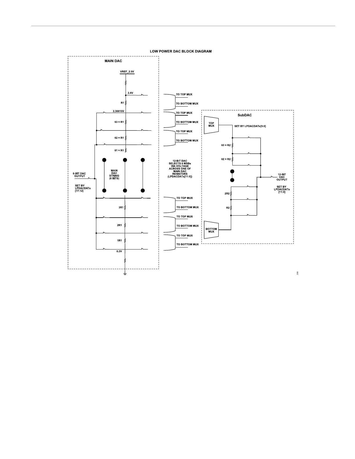
Figure 19. Block Diagram of Low-Power DACs
Low-Power DAC Switch Options
There are a number of switch options available that allow the user
to configure the low-power DACs for various modes of operation.
These switches facilitate a number of different use cases, such
as electrochemical impedance spectroscopy. Figure 16 shows the
location of the switches controlled by LPDACSWx, Bits[4:0]. These
switches are controlled either automatically via LPDACCONx, Bit 5
or individually via the LPDACSWx registers.
When LPDACCONx, Bit 5 is cleared, the switches are configured
for normal mode. SW2 and SW3 are closed and SW0, SW1, and
SW4 are open. When LPDACCONx, Bit 5 is set, the switches
are configured for diagnostic mode. SW0 and SW4 are closed
and SW1, SW2, and SW3 are open. This feature is designed for
electrochemical use cases in normal mode, where the low-power
TIAs are used to measure the sense electrode. In diagnostic mode,
the high-speed TIA is used to measure the sense electrode. By
switching the VZEROx output from the low-power TIA to the high-
speed TIA, the effective bias on the sensor (V
BIAS
to V
ZERO
) is
unaffected. Using the high-speed TIA facilitates high bandwidth
measurements such as impedance, pulse, and cyclic voltammetry.
To control the switches individually, use the LPDACSWx registers.
LPDACSWx, Bit 5 must be set to 1 so that each switch can be
individually controlled via LPDACSWx, Bits[4:0].
Relationship Between 12-Bit and 6-Bit Outputs,
Hardware Compensation Enabled
The 12-bit and 6-bit outputs are mostly independent. However, the
selected 12-bit value does have a loading effect on the 6-bit output
that must be compensated for in user code, particularly when the
12-bit output level is greater than the 6-bit output.
When the 12-bit output < 6-bit output,
12-Bit DAC Output Voltage = 0.2 V + (LPDACDATx,
Bits[11:0] × 0.54 mV)
(7)
 Loading...