Zynq-7000 AP SoC and 7 Series FPGAs MIS v4.1 148
UG586 November 30, 2016
www.xilinx.com
Chapter 1: DDR3 and DDR2 SDRAM Memory Interface Solution
Implementation Details
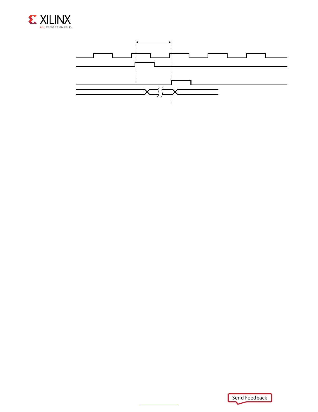
The write_calib_n signal indicating the start of write leveling mode is input to the PHY
control block after tWLDQSEN to ensure that DQS is driven Low after ODT is asserted. In this
mode, periodic write requests must be issued to the PHY control block to generate periodic
DQS pulses for write leveling. During write leveling, PHASER_IN outputs a free-running clock
used to capture the DQ feedback to the DQ IN_FIFOs. During write leveling, the data byte
group IN_FIFOs is in flow-through mode.
Figure 1-65 shows the flow diagram of the sequence of commands during write leveling.
The PHASER_OUT fine phase shift taps are increased one tap at a time to observe a 0-to-1
transition on the feedback DQ. A stable counter is implemented in the write leveling logic to
mitigate the risk of finding a false edge in the jitter region. A counter value of three means
that the sampled data value was constant for three consecutive tap increments and DQS is
considered to be in a stable region with respect to CK. The counter value is reset to 0
whenever a value different from the previous value is detected. Edge detection is inhibited
when the stable counter value is less than 3. The write_calib_n signal is deasserted
when write leveling is performed on all DQSs in all ranks.
X-Ref Target - Figure 1-64
Figure 1-64: Write Leveling Taps Requirement
5'?C??
#,+AT$$23$2!-
$13AT$$23$2!-
$13$ELAYEDWITH
0(!3%2?/547RITE
,EVELING#OMPLETE
$1&EEDBACK
8
!PPROXIMATELYT#+
7ORTHOF4APS2EQUIRED
T#+$$23$2!-#LOCK0ERIOD
 Loading...


