Zynq-7000 AP SoC and 7 Series FPGAs MIS v4.1 147
UG586 November 30, 2016
www.xilinx.com
Chapter 1: DDR3 and DDR2 SDRAM Memory Interface Solution
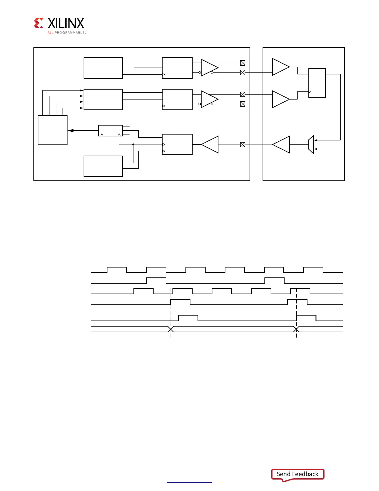
The timing diagram for write leveling is shown in Figure 1-63. Periodic DQS pulses are
output by the FPGA memory interface to detect the level of the CK clock at the DDR3
SDRAM device. The interval between DQS pulses is specified as a minimum of 16 clock
cycles. DQS is delayed using the PHASER_OUT fine and coarse delay in unit tap increments
until a 0 to 1 transition is detected on the feedback DQ input. The DQS delay established by
write leveling ensures the t
DQSS
specification.
Figure 1-64 shows that the worst-case delay required during write leveling can be one tCK
(DDR3 SDRAM clock period).
X-Ref Target - Figure 1-62
Figure 1-62: Write Leveling Block Diagram
$$23$2!-&0'!
$1
#+
#+
$13
$13
/$$2
/$$2
7RITE,EVEL
2EGULAR
&EEDBACK
$1
)3%2$%3
).?&)&/
0(!3%2?).
0(!3%2?/54
)#,+
)#,+$)6
0(!3%2?/54
/#,+?$%,!9%$
$13"53;=
$13"53;=
/#,+
7RITE
,EVELING
,OGIC
#/!23%%.!",%
#/!23%).#
&).%%.!",%
&).%).#
0(9?#,+
"5&'
5'?C??
X-Ref Target - Figure 1-63
Figure 1-63: Write Leveling Timing Diagram
5'?C??
#,+AT&0'!/UTPUT
$13AT&0'!/UTPUT
#+AT$$23$2!-
$13AT$$23$2!-
$1&EEDBACK
$13$ELAYEDWITH
0(!3%2?/UT
8
 Loading...


