Zynq-7000 AP SoC and 7 Series FPGAs MIS v4.1 586
UG586 November 30, 2016
www.xilinx.com
Chapter 4: LPDDR2 SDRAM Memory Interface Solution
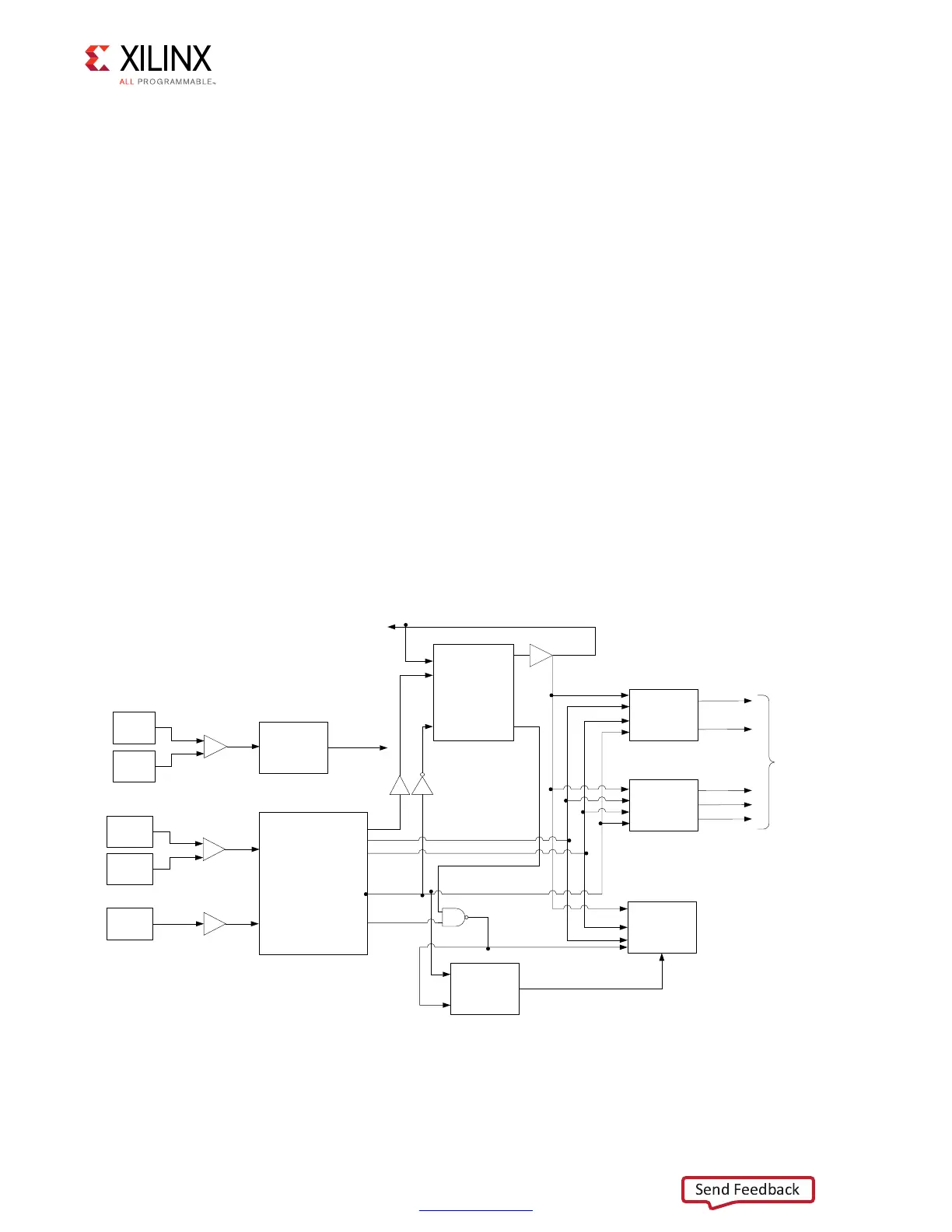
One MMCM and one PLL are required for the PHY. The MMCM is used to generate the
clocks for most of the internal logic, the frequency reference clocks to the phasers, and a
synchronization pulse required for keeping PHY control blocks synchronized in multi-I/O
bank implementations.
For LPDDR2 SDRAM clock frequency range of 200 MHz to 333 MHz, one of the phaser
frequency reference clocks runs at the same frequency as the memory clock and the second
frequency reference clock must be either 2x or 4x the memory clock frequency such that it
meets the range requirement of 400 MHz. The two phaser frequency reference clocks must
be generated by the same MMCM so they are in phase with each other. The block diagram
of the clocking architecture is shown in Figure 4-45.
The default setting for the MMCM multiply (M) and divide (D) values is for the system clock
input frequency to be equal to the memory clock frequency. This 1:1 ratio is not required.
The MMCM input divider (D) can be any value listed in the 7 Series FPGAs Clocking
Resources User Guide (UG472) [Ref 10] as long as the MMCME2_ADV operating conditions
are met and the other constraints listed here are observed. The MMCM multiply (M) value
must be between 1 and 16 inclusive. The MMCM output driver (O) for the memory clock
must be 2. The MMCM VCO frequency range must be kept in the range specified in the
silicon data sheet. The sync_pulse must be 1/16 of the mem_refclk frequency and must
have a duty cycle of 1/16 or 6.25%. For information on physical placement of the MMCM
and the System Clock CCIO input, see Design Guidelines, page 631.
The details of the ISERDES/OSERDES connectivity are shown in Figure 4-50 and Figure 4-52.
X-Ref Target - Figure 4-45
Figure 4-45: Clocking Architecture
CLKREF
N
CLKREF
P
Phaser_IN
Phaser_OUT
PHY Control
0+],'(/$<
5HIHUHQFH&ORFN
IDELAYCTRL
LGHOD\FWUOBUG\
PLL
&/.,1
&/.)%287
/2&.('
&/.)%,1
567
PHASER_REF
&/.,1
567
MMCM
&/.,1
&/.287
/2&.('
567
&/.287
&/.287
&/.287
SYSCLKN
SYSCLKP
6\VWHP&ORFN,QSXW3DLU
SYSRST
,%8)*'6
,%8)
UHIBGOOBORFN
2&/.
2&/.',9
2&/.B'(/$<('
,&/.
,&/.',9
,QWHUQDO)3*$/RJLF&ORFN
%8)*
%8)+
V\QFBSXOVH
PHPBUHIFON
IUHTBUHIFON
,6(5'(626(5'(6
&RQQHFWLYLW\
,%8)*'6
 Loading...


