Reference Manual ADuCM356
SEQUENCER
analog.com Rev. A | 134 of 312
Command Data Control Register
Address: 0x400C21D8, Reset: 0x00000410, Name: CMDDATACON
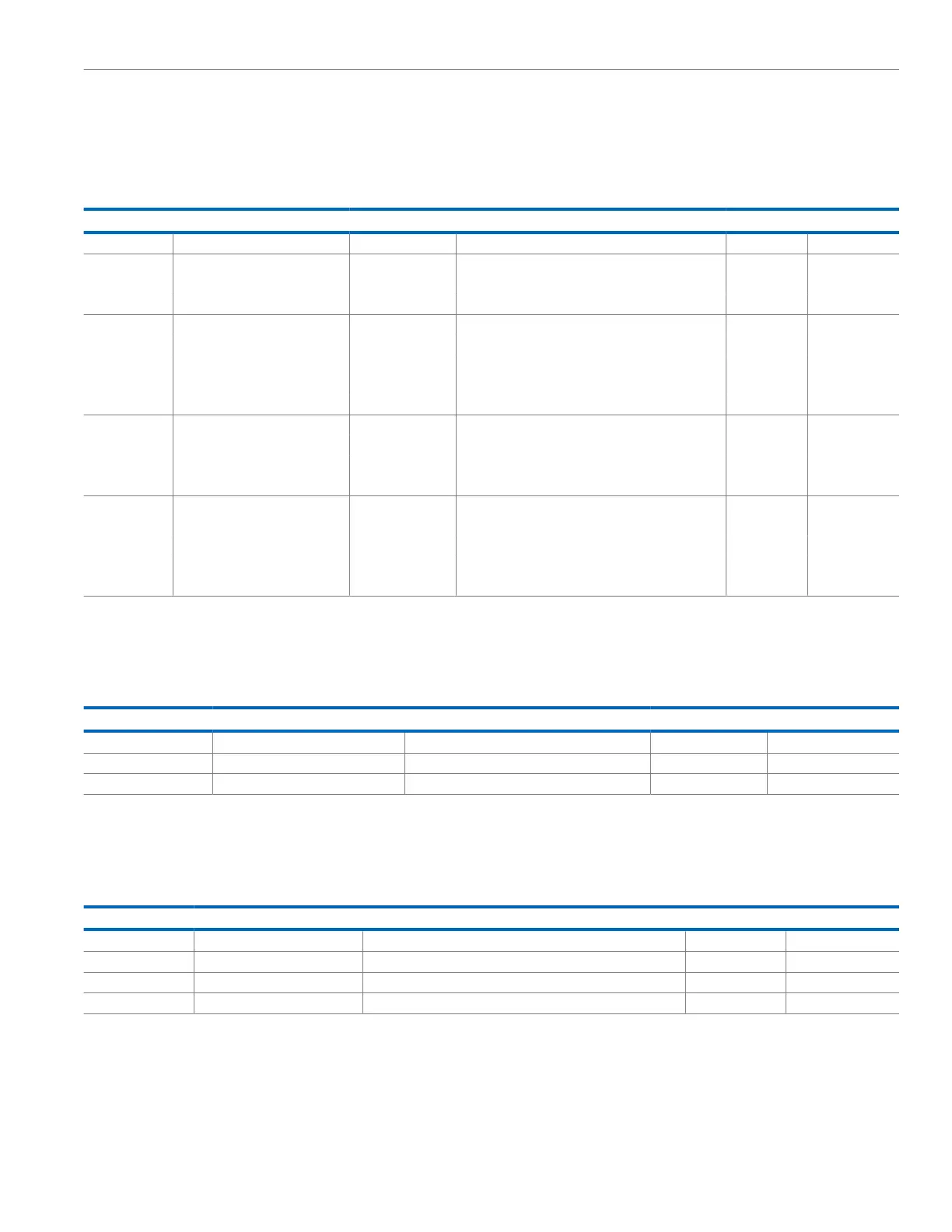
Table 167. Bit Descriptions for CMDDATACON Register
Bits Bit Name Settings Description Reset Access
[31:12] Reserved Reserved. 0x0 R
[11:9] DATAMEMMDE Data FIFO Mode Select. 0x2 R/W
10 FIFO mode.
11 Stream mode.
[8:6] DATA_MEM_SEL Data FIFO Size Select. 0x0 R/W
000 Reserved.
001 2 kB SRAM.
010 4 kB SRAM.
011 6 kB SRAM.
[5:3] CMDMEMMDE Command FIFO Mode. 0x2 R/W
01 Memory mode.
10 Reserved.
11 Reserved.
[2:0] CMD_MEM_SEL Command Memory Select. 0x0 R/W
0x0 Reserved.
0x1 2 kB SRAM.
0x2 4 kB SRAM.
0x3 6 kB SRAM.
Data FIFO Threshold Register
Address: 0x400C21E0, Reset: 0x00000000, Name: DATAFIFOTHRES
Table 168. Bit Descriptions for DATAFIFOTHRES Register
Bits Bit Name Description Reset Access
[31:27] Reserved Reserved. 0x0 R
[26:16] HIGHTHRES High Threshold. 0x0 R/W
[15:0] Reserved Reserved. 0x0 R
Sequence 3 Information Register
Address: 0x400C21E4, Reset: 0x00000000, Name: SEQ3INFO
Table 169. Bit Descriptions for SEQ3INFO Register
Bits Bit Name Description Reset Access
[31:27] Reserved Reserved. 0x0 R
[26:16] INSTNUM SEQ3 Instruction Number. 0x0 R/W
[15:11] Reserved Reserved. 0x0 R
[10:0] STARTADDR SEQ3 Start Address. 0x0 R/W
Sequence 1 Information Register
Address: 0x400C21E8, Reset: 0x00000000, Name: SEQ1INFO

 Loading...