EasyManua.ls Logo

Analog Devices ADuCM356 User Manual

Analog Devices ADuCM356
312 pages
To Next Page IconTo Next Page
To Previous Page IconTo Previous Page
Page #254 background imageLoading...
Page #254 background image
Reference Manual ADuCM356
UART SERIAL INTERFACE
analog.com Rev. A | 254 of 312
FIFO Mode (16550 UART)
The 16-byte deep transmit FIFO and receive FIFO are implement-
ed. Therefore, the UART is compatible with the industry-standard
16550 UART. By default, these FIFOs are disabled. To enable
them, set COMFCR, Bit 0. When enabled, the internal FIFOs allow
16 bytes to be stored in both the receive and transmit modes of
operation, and 3 bits of error data per byte in the receive FIFO.
The interrupt and DMA trigger for the number of bytes received
into the receive FIFO is programmed via COMFCR, Bits[7:6]. The
DMA requests are programmed by the COMFCR, Bit 3. If this bit
is set, the FIFO must also be enabled by setting COMFCR, Bit 0
to 1. If the remaining bytes in a packet are less than the interrupt
trigger number, a timeout interrupt occurs. This timeout is indicated
by COMIIR, Bits[3:1] = 0b110. This timeout period is equal to the
period of four consecutive characters where a single character time
is one start bit, n data bits, one parity bit, and one stop bit, where n
depends on the word length selected by COMLCR, Bits[1:0].
DMA Mode
In DMA mode, user code does not move data to and from the
UART. DMA request signals entering the external DMA block indi-
cate that the UART is ready to transmit or receive data. These DMA
request signals can be disabled in the COMIEN register.
Automatic Baud Rate Detection
The automatic baud detection (ABD) block is used to match the
baud rates of two UART devices automatically. The receiver must
be enabled to detect the mode before a common baud rate is
configured. The COMACR, Bit 0 enables the receiver to work in
ABD mode. A 20-bit counter logic counts the number of cycles
between the programmed rising or falling edge and another rising
or falling edge. An interrupt is generated after the expected edges
are reached. The counter can overflow and generate a timeout
interrupt, such as when there is a continuous break condition or no
expected edges.
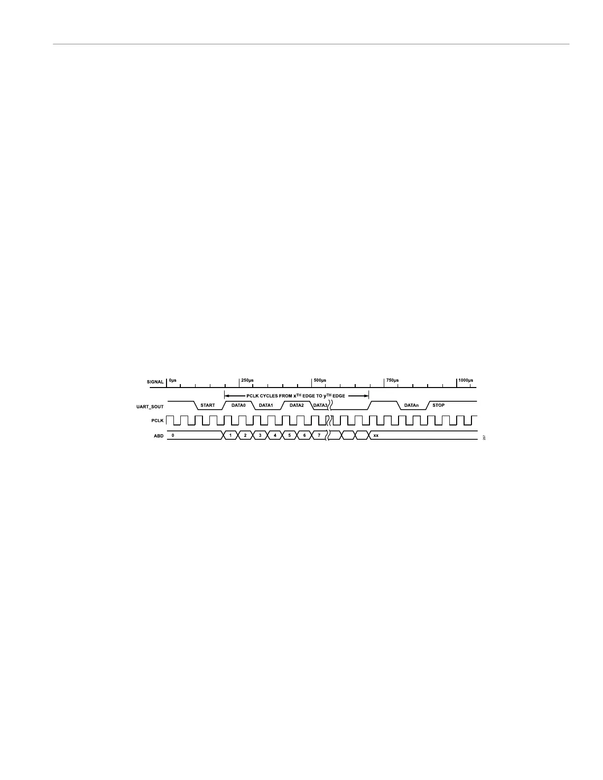
For example, if the data byte being received is 0x0D (0b00001101,
resulting in a carriage return) in 8-bit mode without a parity bit, LSB
first, each bit reads as DATA0 = 1, DATA1 = 0, DATA2 = 1, DATA3 =
1, and DATA4 = DATA5 = DATA6 = DATA7 = 0.
There are three falling edges and three rising edges. The CO-
MACR, Bits[6:4] can be written to 1 decimal (second edge), and
COMACR, Bits[11:8] can be written to 5 decimal (sixth edge) to
count between the first rising edge and the second rising edge. See
Figure 63 for more details.
Figure 63. Autobaud Rate Example
Similarly, for 0x7F (0b01111111, the ASCII DEL value delete key),
COMACR, Bits[6:4] = 1 and COMACR, Bits[11:8] = 3 to count
between the first rising edge and the second rising edge. Automatic
baud rate must be disabled to clear the internal counter and reena-
bled for another sequence (if required). Based on the UART baud
rate configuration, the ABD result can be calculated as follows:
CNT, Bits[19:0] = CountedBits × 2OSR + 2 × COMDIV × (COMFBR,
Bits[12:11] + COMFBR, Bits[10:0]/2048)
where:
CountedBits is the effective number of bits between an active
starting edge and ending edge. It is determined by the application
code on the selected edges and character used for ABD.
COMDIV is calculated as follows:
If CNT, Bits[19:0] < 8 × CountedBits, then OSR = 0, COMDIV =
1, and COMFBR, Bits[10:0] = 512 × CNT, Bits[19:0]/CountedBits −
2048.
If CNT, Bits[19:0] < 16 × CountedBits, then OSR = 1, COMDIV =
1, and COMFBR, Bits[10:0] = 256 × CNT, Bits[19:0]/CountedBits −
2048.
If CNT, Bits[19:0] < 32 × CountedBits, then OSR = 2, COMDIV =
1, and COMFBR, Bits[10:0] = 128 × CNT, Bits[19:0]/CountedBits −
2048.
If CNT, Bits[19:0] ≥ 32 × CountedBits, then OSR = 3.
If CNT, Bits[19:0] is exactly divided by 32 × CountedBits, then
COMDIV = (CNT, Bits[19:0]/32)/CountedBits.
Otherwise, COMDIV = 2log
2
((CNT[19:0]/32)/CountedBits) and
COMFBR, Bits[10:0] = (((64 × CNT, Bits[19:0])/COMDIV)/ Counted-
Bits) − 2048.
To reduce truncation error, the DIVM field (COMFBR, Bits[12:11]) is
set to 1. The DIV field (COMDIV, Bits[15:0]) is set to the nearest
power of 2. COMASRH, Bits[7:0] and COMASRL, Bits[15:4] make
up CNT, Bits[19:0].
Clock Gating
The clock driving the UART logic is automatically gated off when
idle, and not accessed. This automatic clock gating cannot be
disabled by COMCTL, Bit 1.

Table of Contents

Question and Answer IconNeed help?

Do you have a question about the Analog Devices ADuCM356 and is the answer not in the manual?

Analog Devices ADuCM356 Specifications

General IconGeneral
BrandAnalog Devices
ModelADuCM356
CategoryMicrocontrollers
LanguageEnglish

Summary

PREFACE

SCOPE

Provides a detailed description of the functionality and features of the ADuCM356.

CLOCKING ARCHITECTURE

DIGITAL DIE CLOCK FEATURES

Details the clock sources, dividers, and gating for the digital die system clock.

ANALOG DIE CLOCK FEATURES

Details the clock sources, dividers, and gating for the analog die system clock.

POWER MANAGEMENT UNIT

Active Mode

Describes the fully active operating mode where the Arm Cortex-M3 executes from flash and SRAM.

Flexi Mode

Describes the mode where the Arm Cortex-M3 is disabled, allowing peripherals to operate.

Hibernate Mode

Describes the low-power mode where the digital core and most analog blocks are powered down.

SYSTEM RESETS

DIGITAL DIE RESET OPERATION

Explains the reset sources and operation for the digital die, including software resets.

PROGRAMMING, PROTECTION, AND DEBUG

Debug Features

Details the SWD port, flash patch breakpoints, and data watchpoint/trigger units for debugging.

SYSTEM EXCEPTIONS AND PERIPHERAL INTERRUPTS

CORTEX-M3 AND FAULT MANAGEMENT

Describes the system exceptions and fault handling features integrated with the Cortex-M3 processor.

ANALOG DIE CIRCUITRY SUMMARY

ADC, HIGH-SPEED DAC, AND ASSOCIATED AMPLIFIERS OPERATING MODE CONFIGURATION

Configures the operating modes for ADC, High-Speed DAC, and associated amplifiers.

ADC CIRCUIT

ADC CIRCUIT FEATURES

Lists the key features of the ADuCM356's fast multichannel, 16-bit ADC.

LOW-POWER POTENTIOSTAT AMPLIFIERS AND LOW-POWER TIAS

LOW-POWER POTENTIOSTAT AMPLIFIERS

Details the two low-power potentiostat amplifiers for setting external sensor bias voltage.

HIGH-SPEED DAC CIRCUITS

HIGH-SPEED DAC OUTPUT SIGNAL GENERATION

Explains how to generate high-speed DAC output voltage via direct write or waveform generator.

PROGRAMMABLE SWITCHES CONNECTING THE EXTERNAL SENSOR TO THE HIGH-SPEED DAC AND HIGH-SPEED TIA

DX SWITCHES

Selects pins for the high-speed DAC excitation amplifier output, used for impedance measurements.

SEQUENCER

SEQUENCER COMMANDS

Describes the two types of commands: write commands and timer commands (wait, timeout).

SLEEP AND WAKE-UP TIMER

CONFIGURING A DEFINED SEQUENCE ORDER

Defines the order of sequence execution periodically using the SEQORDER register.

USE CASE CONFIGURATIONS

HIBERNATE MODE WHILE MAINTAINING A DC BIAS TO THE SENSOR

Details setup for hibernate mode while maintaining sensor bias voltage.

DMA CONTROLLER

DMA FEATURES

Lists the features of the ADuCM356's dedicated and independent DMA channels.

FLASH CONTROLLER

SUPPORTED COMMANDS

Summarizes the commands supported by the flash controller for read, write, erase, and signature operations.

REGISTER DETAILS: FLASH CACHE CONTROLLER (FLCC)

COMMAND REGISTER

Allows execution of specified flash commands like write, erase, abort, and signature generation.

DIGITAL INPUTS AND OUTPUTS

DIGITAL INPUTS AND OUTPUTS OPERATION

Explains how to configure, read, and write digital input and output pins.

I2C SERIAL INTERFACE

I2C OPERATION

Details the steps required to run the I2C peripheral, including startup and modes.

SERIAL PERIPHERAL INTERFACES

SPI OPERATION

Describes the operation of the SPI interface, including initiator and target modes.

REGISTER SUMMARY: SPI0/SPI1

STATUS REGISTERS

Provides status information for SPI0 and SPI1, including ready, overflow, and error conditions.

REGISTER DETAILS: UART

INTERRUPT ENABLE REGISTER

Configures which interrupt sources generate an interrupt for the UART.

DIGITAL DIE GENERAL-PURPOSE TIMERS

GENERAL-PURPOSE TIMER OPERATIONS

Explains the operation of timers in free running mode and periodic mode.

REGISTER SUMMARY: ANALOG DIE GENERAL-PURPOSE TIMERS

CONTROL REGISTER

Controls timer operation, including clock source, mode, and event selection.

REGISTER DETAILS: DIGITAL DIE WAKE-UP TIMER

STATUS 0 REGISTER

Provides status information for WUT operation, including synchronization and pending writes.

CYCLIC REDUNDANCY CHECK

CRC OPERATING MODES

Details the core access and DMA access modes for CRC calculation.

REGISTER SUMMARY: CRC

CRC CONTROL REGISTER

Controls the CRC peripheral, including enabling, mirroring, and calculation order.

HARDWARE DESIGN CONSIDERATIONS

SERIAL WIRE DEBUG INTERFACE

Describes the SWD interface for debugging and programming, replacing JTAG.