EasyManua.ls Logo

RHK Technology R9 - Block Diagram of Output Circuitry; Property Panel in Hardware Space; Figure B.2. Block Diagram of Drive 1 and Drive 2 Output Circuitry; Figure B.3. Channel 1 Drive - Property Panel in Hardware Space

Default Icon
230 pages
Print Icon
To Next Page IconTo Next Page
To Previous Page IconTo Previous Page
Loading...
Hardware Space Components
74
The CH 1 Drive and CH 2 Drives also are output on the Preamp connector. These outputs are 100 Ω
differential outputs that are designed to work with RHK’s external preamplifiers and signal conditioners.
For details on interfacing customer circuitry to these differential inputs, contact support@rhk-tech.com.
Table B.1. Channel 1 Drive Output
Output Location
Output Type
Bandwidth
Example Application
R9 Rear Panel BNC
±1 V 50 Ω
10 MHz
AFM - Probe Drive
IVP-R9 BNC
±10 V
50 kHz
STM - Sample Bias
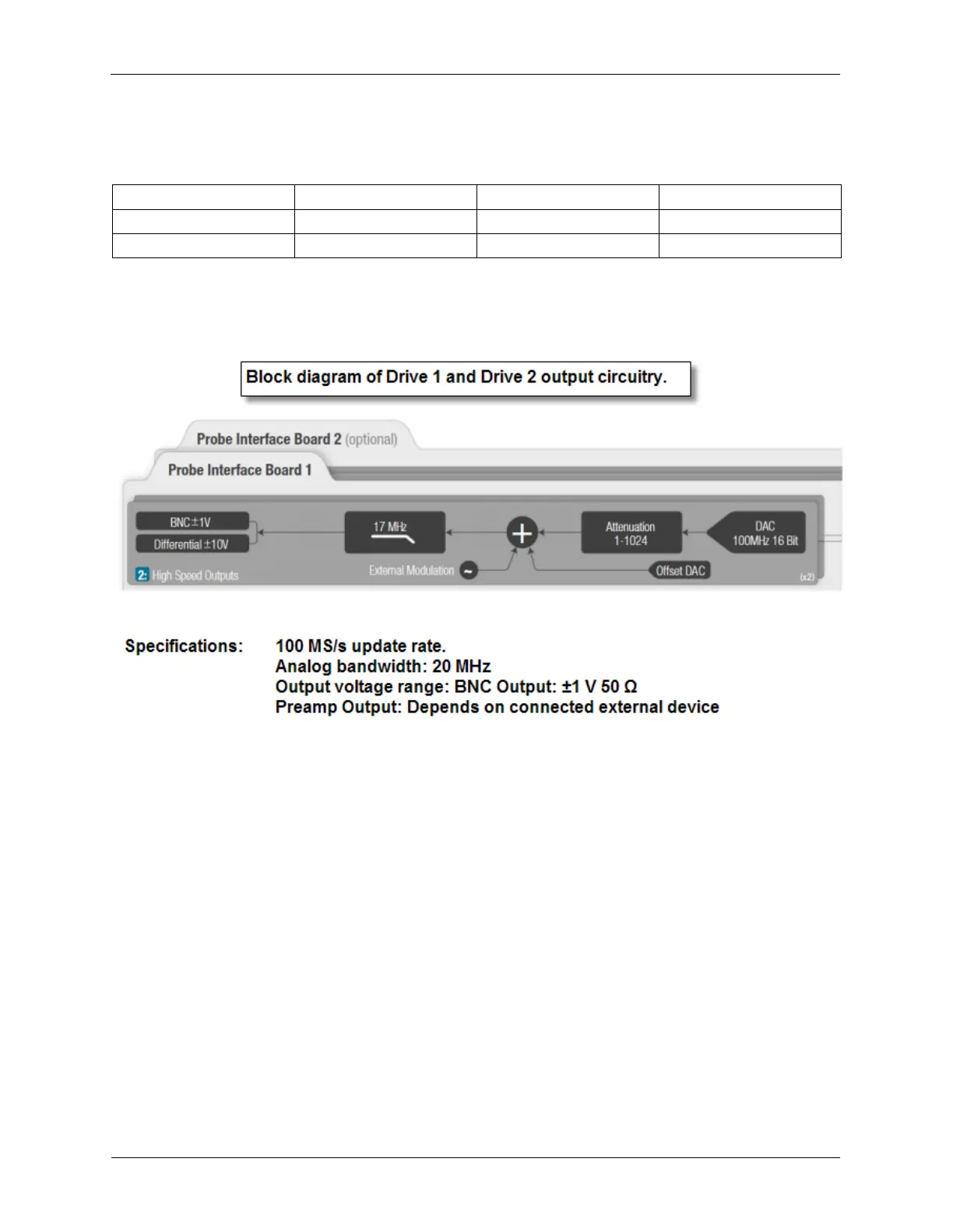
B.1.2. Block Diagram of Output Circuitry
Figure B.2. Block Diagram of Drive 1 and Drive 2 Output Circuitry
B.1.3. Property Panel in Hardware Space
Figure B.3. Channel 1 Drive - Property Panel in Hardware Space

Table of Contents