Hardware Space Components
The Offset Enable (3) check box enables the Offset DAC to be added to the input signal. This is one of
the few analog summing junctions in the R9 controller. This summing junction adds approximately 1 nV of
noise to the input signal. This can be safely ignored by almost every experiment as it is far below the
noise floor of most experiments. The parameter is provided for the customer working in the mK range
where the absolutely lowest noise level is desired. For other users, the radio button should be checked to
allow the offset to be used to null out any input offset errors.
The Input Gain (4) dropdown box allows the input signal to be amplified before it is digitized. This can
improve the resolution of the measurement as more of the full scale range of the ADC will be utilized. The
gain can be increased by factors of 2 from 1 to 512. The full bandwidth of 20 MHz is maintained
throughout the entire gain range.
The Coupling (5) dropdown box selects between DC and AC coupling. When performing STM
measurements and contact AFM measurements, the Coupling is set to DC. When performing non-
contact AFM measurements, the Coupling is set to AC.
The Full Scale (6) information box displays the maximum signal that the ADC is able to measure. When
the input gain is set to 1, this Full Scale is equal to the full scale input range of the ADC. As the input gain
is increased, the Full Scale that can be measured is reduced by the amount of the gain. For example, if
the full scale input of the ADC is 1V and the input gain is set to 1, the ADC will be able to measure a
signal in the range of ±1V. When the input gain is increased to 8, the ADC will now be able to measure a
signal in the range of ±0.125V.
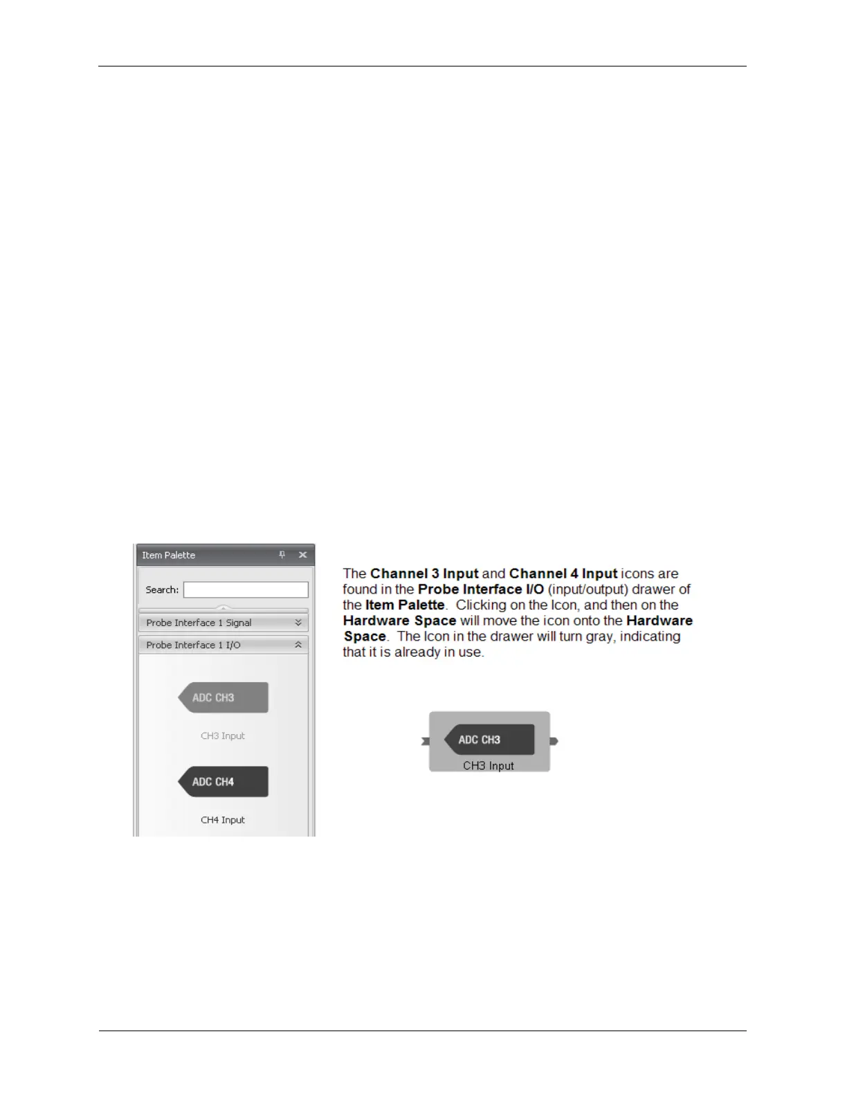
B.3. Channel 3 Input and Channel 4 Input
B.3.1. Hardware Space
Figure B.7. Hardware Space - Channel 3 Input
B.3.2. Block Diagram of Input Circuitry
Figure B.8. Block Diagram of Channel 3 and Channel 4 Input Circuitry