Zynq-7000 AP SoC and 7 Series FPGAs MIS v4.1 241
UG586 November 30, 2016
www.xilinx.com
Chapter 1: DDR3 and DDR2 SDRAM Memory Interface Solution
dbg_wcal_mux_rd_rise0_r
Data pattern received on the Write Calibration stage MUX on rising
edge 0.
dbg_wcal_mux_rd_fall0_r
Data pattern received on the Write Calibration stage MUX on falling
edge 0.
dbg_wcal_mux_rd_rise1_r
Data pattern received on the Write Calibration stage MUX on rising
edge 1.
dbg_wcal_mux_rd_fall1_r
Data pattern received on the Write Calibration stage MUX on falling
edge 1.
dbg_wcal_mux_rd_rise2_r
Data pattern received on the Write Calibration stage MUX on rising
edge 2.
dbg_wcal_mux_rd_fall2_r
Data pattern received on the Write Calibration stage MUX on falling
edge 2.
dbg_wcal_mux_rd_rise3_r
Data pattern received on the Write Calibration stage MUX on rising
edge 3.
dbg_wcal_mux_rd_fall3_r
Data pattern received on the Write Calibration stage MUX on falling
edge 3.
dbg_early1_data_match_r
Asserts when the pattern detected is one CK clock cycle early and a
match is found during Write Calibration.
dbg_early2_data_match_r
Asserts when the pattern detected is two CK clock cycle early and a
match is found during Write Calibration.
dbg_wcal_sanity_pat_data_match_valid_r
Asserts when the valid pattern is detected on the data and is found to
match with the expected pattern sent during Write Calibration sanity
check.
dbg_prbs_final_dqs_tap_cnt_r Tap values set at the end of PRBS Read Leveling stage.
dbg_prbs_first_edge_taps
Tap value when the first edge is found during PRBS Read Leveling
stage calibration.
dbg_prbs_second_edge_taps
Tap value when the second edge is found during PRBS Read Leveling
stage calibration.
dbg_ocal_center_calib_done OCLKDELAY center calibration completing indicator.
dbg_phy_oclkdelay_cal_taps
Final stage 3 tap values for all the bytes in the interface. Bits[5:0] for
byte 0 and Bits[11:6] for byte 1.
dbg_ocal_tap_cnt Stage 3 tap value during calibration for each group.
VIO Signals (Control)
dbg_bit Currently Unused
dbg_dqs
Input to select DQS byte for which the ILA displays the tap counts of
PHASER_OUT. For example, set to 4'b0000 to view the results on
DQS[0].
vio_modify_enable See Table 1-83.
vio_data_mode_value See Table 1-83.
vio_addr_mode_value See Table 1-83.
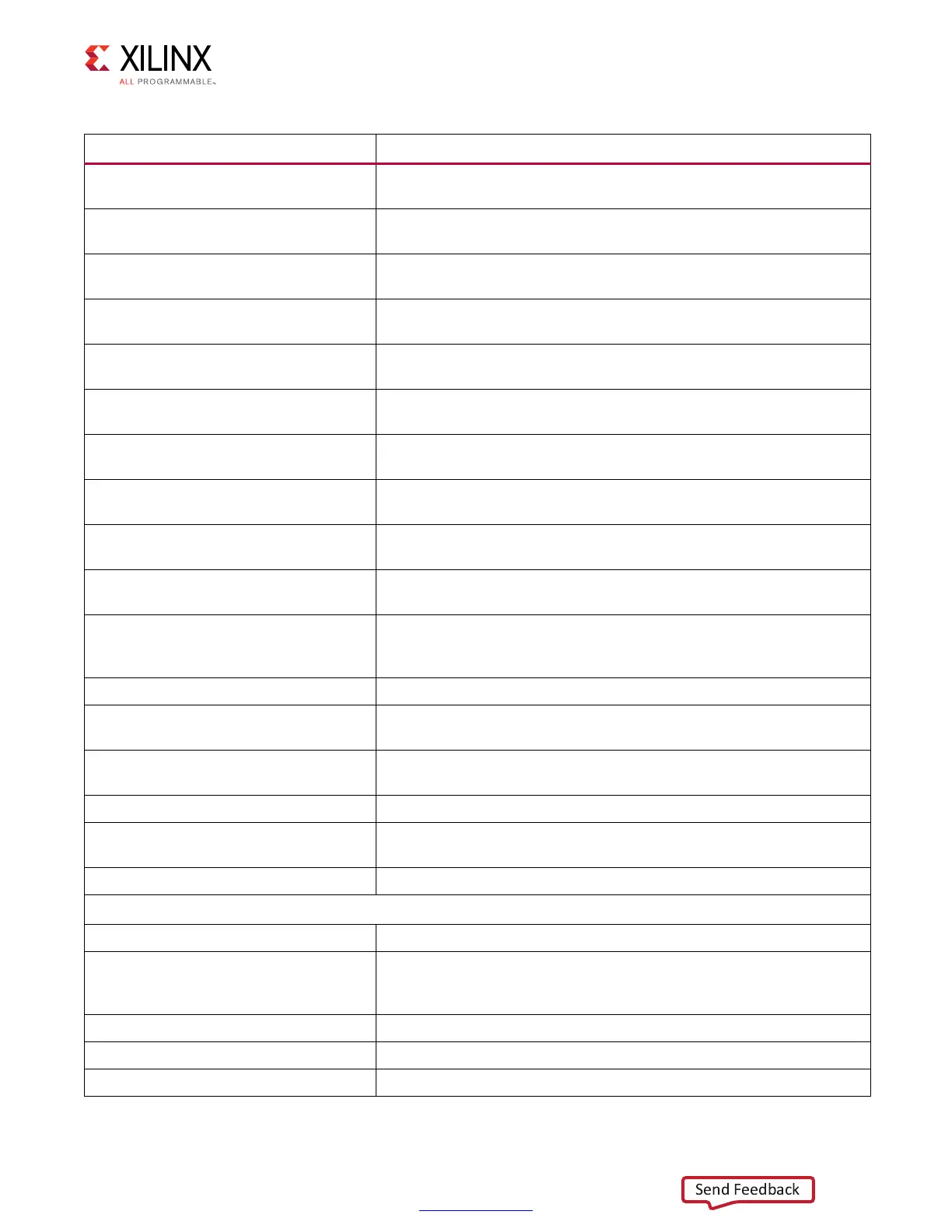
Table 1-74: DDR2/DDR3 Debug Signals (Cont’d)
Signal Name Description
 Loading...


