Zynq-7000 AP SoC and 7 Series FPGAs MIS v4.1 438
UG586 November 30, 2016
www.xilinx.com
Chapter 3: RLDRAM II and RLDRAM 3 Memory Interface Solutions
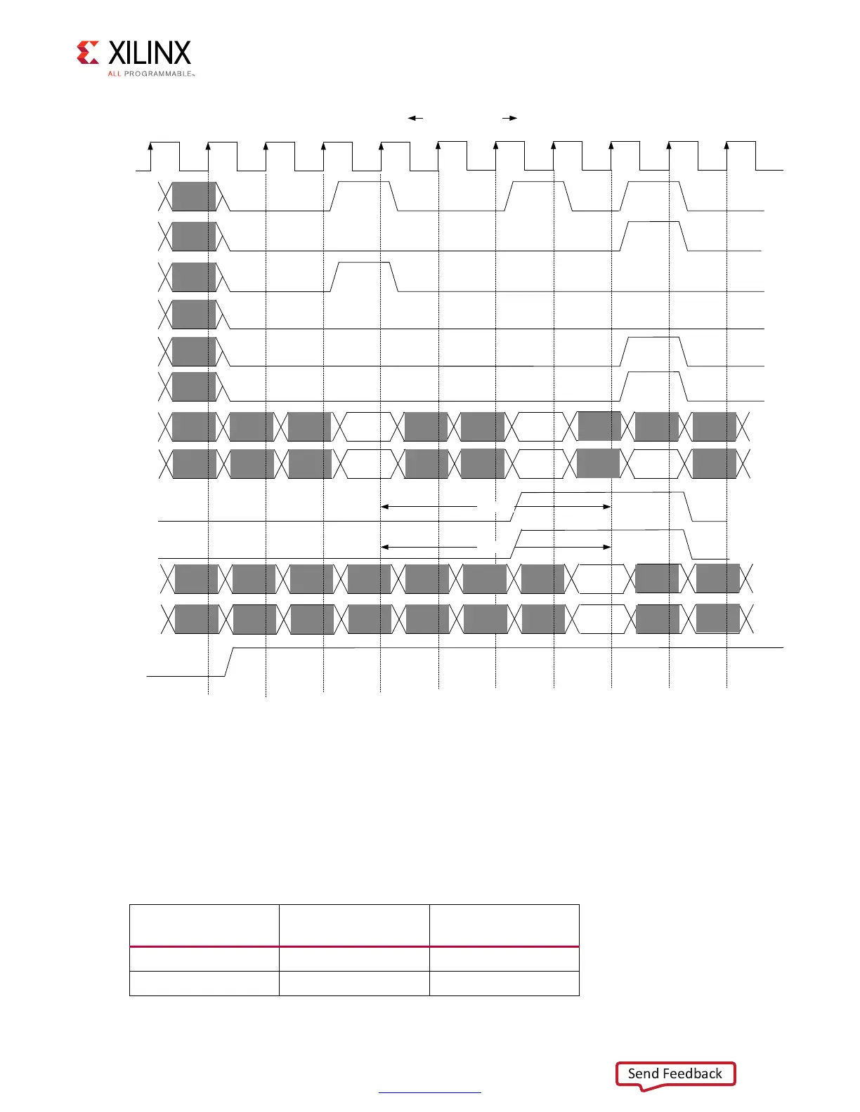
The controller sends the wr_en signals and data at the necessary time based on the
configuration setting. This time changes depending on the configuration. Table 3-13 details
when the wr_en signals should be asserted with the data valid for a given configuration. If
address multiplexing is used, the PHY handles rearranging the address signals and
outputting the address over two clock cycles rather than one.
X-Ref Target - Figure 3-46
Figure 3-46: PHY-Only Interface for RLDRAM II Burst Length 4, Configuration 3, and Address
Multiplexing OFF
#,+
MC?CS ;=
[./0
!]
MC?WE;=
MC?REF ;=
MC?WE;=
MC?WR ?DATA
MC?CS ;=
[./0
!]
MC?WR ?DM
MC?REF ;=
)NIT ?CALIB ?
COMPLETE
MC?ADDR
[./0
"!]
[./0
"!]
MC?BA
MC?WR ?EN;=
MC?WR ?EN;=
7RITE
#OMMAND
2EAD
#OMMAND
2EFRESH
#OMMAND
["!
"!]
[WD
WD]
[W?DM
W?DM]
CLOCKS
CLOCKS
3WITCHTHEBUS
8
Table 3-13: RLDRAM II Command to Write Enable Timing
Address Multiplexing Configuration
Command to Write
Enable (Clock Cycles)
ON 1 3
24
 Loading...


