EasyManua.ls Logo

Analog Devices ADuCM356 User Manual

Analog Devices ADuCM356
312 pages
To Next Page IconTo Next Page
To Previous Page IconTo Previous Page
Page #156 background imageLoading...
Page #156 background image
Reference Manual ADuCM356
USE CASE CONFIGURATIONS
analog.com Rev. A | 156 of 312
Step 2: Measure R
LOAD02
and External Sensor
(R
SENSOR
)
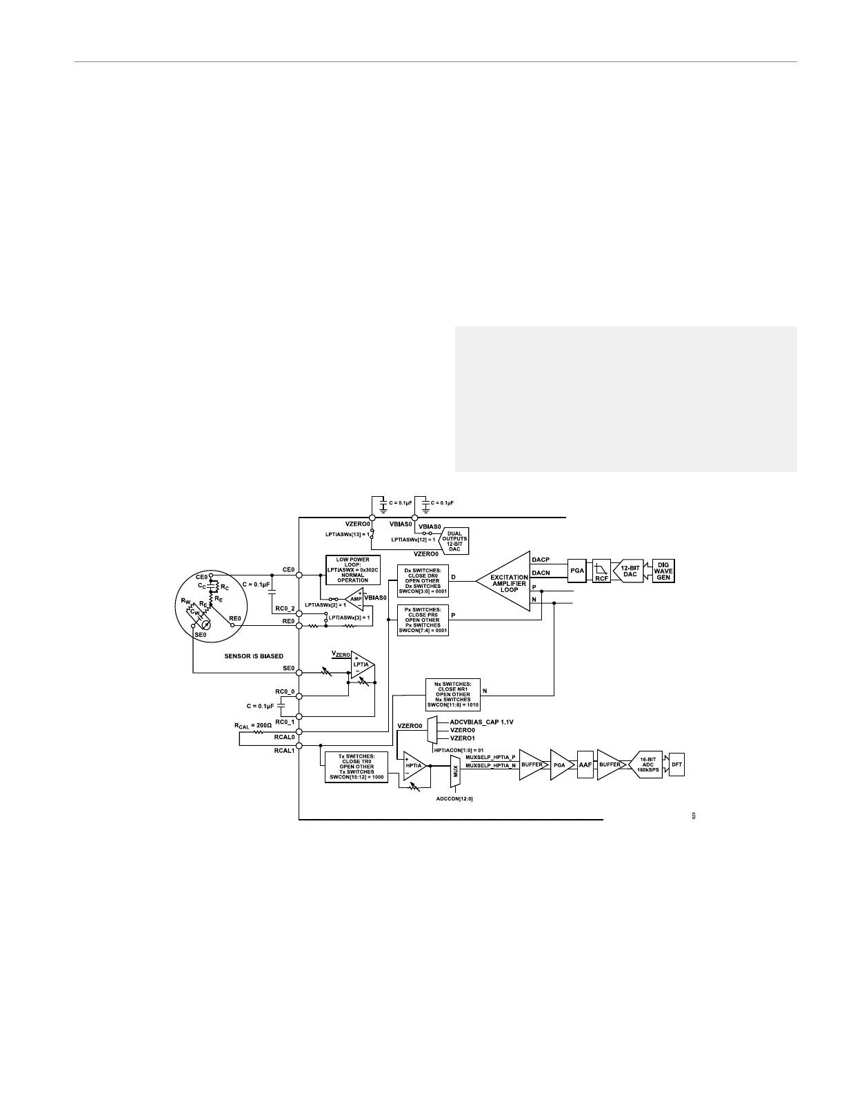
The electrochemical sensor remains biased during this step, but the
working electrode voltage is set by the high-speed TIA instead of
the low-power TIA.
The R
LOAD02
is a fixed value load resistor (100 Ω). In Figure 41,
the reference electrode is the sensor impedance. The waveform
generator and the high-speed DAC generate a 10 mV amplitude
sine waveform on the DC bias voltage that is required for the
reference electrode and the sensing electrode sensor nodes. DACN
is the bias voltage input to the excitation loop from the high-speed
DAC. The sine wave generated by the high-speed DAC is added
at the DACP node. N, P, DACN, and DACP are four inputs of the
excitation amplifier. The differential voltage between the P node and
the N node is the same as the differential voltage between DACP
and DACN.
The sensor is biased, meaning that the required DC voltage is
applied between the reference electrode and the working electrode.
The AC signal is added to the sensor, and the DC bias voltage
is also maintained. The D node provides the correct voltage and
current. As such, the stimulus sine waveform is added between
the electrochemical sensor reference electrode and the high-speed
TIA input. The reference electrode + R
LOAD02
is included in this
AC excitation loop. At this point, the high-speed TIA output is
measured via the ADC signal chain. The programmed number of
ADC samples are fed to the DFT block, which outputs a complex
number (real or imaginary) that reflects the DFT result for the
ADC measurements of the reference electrode + R
LOAD02
. By using
the RCAL impedance measurement result determined after Step 4
and ratiometric measurements, it is possible to obtain an accurate
reference electrode + R
LOAD02
impedance value.
Configure the Tx, Dx, Nx, and Px switches appropriately, as per the
following example code:
AfeSâ–º
witchDPNT(SWID_D5_CE0,SWID_P5_RE0,SWID_N5_SE0RL
OAD,SWID_T5_SE0RLOAD|SWID_T9);
// Connect Excitation Amplifier D to the LP
// Connect Excitation Amplifier P to RE0
// Connect Excitation Amplifier N to SE0 via
RLOAD02
// Connect HSTIA to SE0 via RLOAD02. Close T9
Figure 41. Step Three of Impedance Measurement, R
LOAD02
+ R
SENSOR
Measurement
Step 3: Measure R
LOAD02
The counter electrode and reference electrode of the electrochem-
ical sensor are floating during this stage of the measurement
sequence.
The main differences between Step 2 and Step 3 are as follows:
â–º The reference electrode is disconnected from the excitation
amplifier P node.
â–º The counter electrode is disconnected from the excitation amplifi-
er D node and is connected directly to R
LOAD02
.
â–º The excitation amplifier D node is connected to the working
electrode node.
Therefore, the excitation signal is applied to R
LOAD02
and the
sensor is floating, as shown in Figure 42. The AC excitation loop D
node, P node, and R
LOAD02
are shorted. The AC excitation loop N
node, TIA T node, and R
LOAD02
are shorted. Measure the stimulus

Table of Contents

Question and Answer IconNeed help?

Do you have a question about the Analog Devices ADuCM356 and is the answer not in the manual?

Analog Devices ADuCM356 Specifications

General IconGeneral
BrandAnalog Devices
ModelADuCM356
CategoryMicrocontrollers
LanguageEnglish

Summary

PREFACE

SCOPE

Provides a detailed description of the functionality and features of the ADuCM356.

CLOCKING ARCHITECTURE

DIGITAL DIE CLOCK FEATURES

Details the clock sources, dividers, and gating for the digital die system clock.

ANALOG DIE CLOCK FEATURES

Details the clock sources, dividers, and gating for the analog die system clock.

POWER MANAGEMENT UNIT

Active Mode

Describes the fully active operating mode where the Arm Cortex-M3 executes from flash and SRAM.

Flexi Mode

Describes the mode where the Arm Cortex-M3 is disabled, allowing peripherals to operate.

Hibernate Mode

Describes the low-power mode where the digital core and most analog blocks are powered down.

SYSTEM RESETS

DIGITAL DIE RESET OPERATION

Explains the reset sources and operation for the digital die, including software resets.

PROGRAMMING, PROTECTION, AND DEBUG

Debug Features

Details the SWD port, flash patch breakpoints, and data watchpoint/trigger units for debugging.

SYSTEM EXCEPTIONS AND PERIPHERAL INTERRUPTS

CORTEX-M3 AND FAULT MANAGEMENT

Describes the system exceptions and fault handling features integrated with the Cortex-M3 processor.

ANALOG DIE CIRCUITRY SUMMARY

ADC, HIGH-SPEED DAC, AND ASSOCIATED AMPLIFIERS OPERATING MODE CONFIGURATION

Configures the operating modes for ADC, High-Speed DAC, and associated amplifiers.

ADC CIRCUIT

ADC CIRCUIT FEATURES

Lists the key features of the ADuCM356's fast multichannel, 16-bit ADC.

LOW-POWER POTENTIOSTAT AMPLIFIERS AND LOW-POWER TIAS

LOW-POWER POTENTIOSTAT AMPLIFIERS

Details the two low-power potentiostat amplifiers for setting external sensor bias voltage.

HIGH-SPEED DAC CIRCUITS

HIGH-SPEED DAC OUTPUT SIGNAL GENERATION

Explains how to generate high-speed DAC output voltage via direct write or waveform generator.

PROGRAMMABLE SWITCHES CONNECTING THE EXTERNAL SENSOR TO THE HIGH-SPEED DAC AND HIGH-SPEED TIA

DX SWITCHES

Selects pins for the high-speed DAC excitation amplifier output, used for impedance measurements.

SEQUENCER

SEQUENCER COMMANDS

Describes the two types of commands: write commands and timer commands (wait, timeout).

SLEEP AND WAKE-UP TIMER

CONFIGURING A DEFINED SEQUENCE ORDER

Defines the order of sequence execution periodically using the SEQORDER register.

USE CASE CONFIGURATIONS

HIBERNATE MODE WHILE MAINTAINING A DC BIAS TO THE SENSOR

Details setup for hibernate mode while maintaining sensor bias voltage.

DMA CONTROLLER

DMA FEATURES

Lists the features of the ADuCM356's dedicated and independent DMA channels.

FLASH CONTROLLER

SUPPORTED COMMANDS

Summarizes the commands supported by the flash controller for read, write, erase, and signature operations.

REGISTER DETAILS: FLASH CACHE CONTROLLER (FLCC)

COMMAND REGISTER

Allows execution of specified flash commands like write, erase, abort, and signature generation.

DIGITAL INPUTS AND OUTPUTS

DIGITAL INPUTS AND OUTPUTS OPERATION

Explains how to configure, read, and write digital input and output pins.

I2C SERIAL INTERFACE

I2C OPERATION

Details the steps required to run the I2C peripheral, including startup and modes.

SERIAL PERIPHERAL INTERFACES

SPI OPERATION

Describes the operation of the SPI interface, including initiator and target modes.

REGISTER SUMMARY: SPI0/SPI1

STATUS REGISTERS

Provides status information for SPI0 and SPI1, including ready, overflow, and error conditions.

REGISTER DETAILS: UART

INTERRUPT ENABLE REGISTER

Configures which interrupt sources generate an interrupt for the UART.

DIGITAL DIE GENERAL-PURPOSE TIMERS

GENERAL-PURPOSE TIMER OPERATIONS

Explains the operation of timers in free running mode and periodic mode.

REGISTER SUMMARY: ANALOG DIE GENERAL-PURPOSE TIMERS

CONTROL REGISTER

Controls timer operation, including clock source, mode, and event selection.

REGISTER DETAILS: DIGITAL DIE WAKE-UP TIMER

STATUS 0 REGISTER

Provides status information for WUT operation, including synchronization and pending writes.

CYCLIC REDUNDANCY CHECK

CRC OPERATING MODES

Details the core access and DMA access modes for CRC calculation.

REGISTER SUMMARY: CRC

CRC CONTROL REGISTER

Controls the CRC peripheral, including enabling, mirroring, and calculation order.

HARDWARE DESIGN CONSIDERATIONS

SERIAL WIRE DEBUG INTERFACE

Describes the SWD interface for debugging and programming, replacing JTAG.