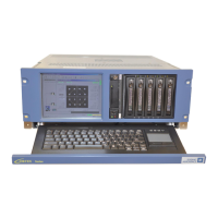
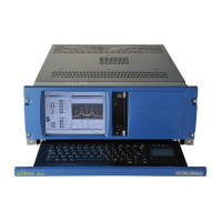
HIGH DATA RATE RECEIVER
HDR-4G+ USER’S MANUAL
Ref. DTU 100782
Is.Rev 3.5
Date: June 1, 2021
© Safran Data Systems – IMP000074 e14r1
This document is the property of Safran Data Systems.
It cannot be duplicated or distributed without expressed written consent.
Figure 52: 8 DPU Data Flow for automatic ambiguity resolution ..................................................................................... 144
Figure 53: Data Generation Scheme .................................................................................................................................. 155
Figure 54: 10-bit generator with feedbacks after register 3 and 0 ..................................................................................... 156
Figure 55: Frame aligned with File ................................................................................................................................... 158
Figure 56: 16APSK Mapping 1 ......................................................................................................................................... 162
Figure 57: 16APSK Mapping 2 ......................................................................................................................................... 162
Figure 58: Example of 2 DGUs merging for simulation of independent I/Q transmission in QPSK ................................ 165
Figure 59: Example of 3 DGUs merging for simulation of independent I/Q/C transmission in 8PSK ............................. 166
Figure 60: Example of 3 DGUs with different offsets ....................................................................................................... 166
Figure 61: IF Signal Generation ........................................................................................................................................ 168
Figure 62: GUI: IF Unit ..................................................................................................................................................... 169
Figure 63: Example 1: 2 adjacent channels on IF1 – 1 single channel on IF2 .................................................................. 170
Figure 64: Example 1: 2 adjacent channels on IF1 – 1 single channel on IF2 (GUI) ........................................................ 170
Figure 65: Example 2: 3 adjacent channels on IF1 – Nothing on IF2 ............................................................................... 171
Figure 66: Example 2: 3 adjacent channels on IF1 – Nothing on IF2 (GUI) ..................................................................... 171
Figure 67: Example 3: 1 channel on IF1 – 1 channel on IF2 ............................................................................................. 172
Figure 68: Example 3: 1 channel on IF1 – 1 channel on IF2 (GUI) .................................................................................. 172
Figure 69: ECL inputs on test modulator board – Single Ended ECL ............................................................................... 173
Figure 70: ECL inputs on test modulator board - Differential ECL .................................................................................. 173
Figure 71: IQZ mapping example...................................................................................................................................... 175
Figure 72: direct modulator input, as seen in the main modulator window ....................................................................... 176
Figure 73: 100 Mbps, QPSK direct input setting ............................................................................................................... 177
Figure 74: Example of Non-linearity in a RG188A/U Cable ............................................................................................ 179
Figure 75: Example of cable compensation ....................................................................................................................... 180
Figure 76: SPS Start Sequence .......................................................................................................................................... 187
Figure 77: CTX Document Management .......................................................................................................................... 189
Figure 78: MCS Menu Management Window .................................................................................................................. 190
Figure 79: About CORTEX SPS Version.......................................................................................................................... 202
Figure 80: MCS Start Sequence ........................................................................................................................................ 212
Figure 81: MCS Top-Level Window ................................................................................................................................. 215
Figure 82: MCS Login Window ........................................................................................................................................ 215
Figure 83: Multiple Tabbed Document Interface .............................................................................................................. 216
Figure 84: Cortex MCS About: Software Version ............................................................................................................ 224
Figure 85: Changing a Password ....................................................................................................................................... 225
Figure 86: Graphical User Interface: Windows Breakdown .............................................................................................. 233
Figure 87: CORTEX HDR: Global Window .................................................................................................................... 234
Figure 88: Global Engineering Window ............................................................................................................................ 236
Figure 89: TCP-IP Secondary Window ............................................................................................................................. 237
Figure 90: CORTEX « Time » Window ............................................................................................................................ 238
Figure 91: Leap Second Management ............................................................................................................................... 241
Figure 92: CORTEX
HDR: Config. Window .................................................................................................................... 244
Figure 93: Configuration help Window for the Demodulator ........................................................................................... 246
Figure 94: Configuration help Window for the Test Modulator ........................................................................................ 246
Figure 95: CORTEX HDR: Project Window .................................................................................................................... 248
Figure 96: CORTEX HDR: Information Window............................................................................................................. 249
Figure 97: "Mod" Window ................................................................................................................................................ 250
Figure 98: "ModCnf" Window .......................................................................................................................................... 251
Figure 99: Demodulator: Global Window for QPSK Modulation + I & D Filter .............................................................. 252
Figure 100: Demodulator: Global Window for QPSK Modulation + Raised Cosine Filter .............................................. 252
Figure 101: Demodulator: Global Window for QPSK Modulation + Custom Filter......................................................... 253
Figure 102: Demodulator: Global Window for OQPSK Modulation ................................................................................ 253
Figure 103: Demodulator: Global Window for GMSK Modulation ................................................................................. 254
Figure 104: Demodulator: Global Window for SOQPSK Modulation .............................................................................. 254
Figure 105: Demodulator: Global Window for UQPSK Modulation ................................................................................ 255
Figure 106: Demodulator: Global Window for 8PSK Modulation .................................................................................... 255
Figure 107: Demodulator: Global Window for 16QAM Modulation ................................................................................ 256
Figure 108: Demodulator: Global Window for 16APSK Modulation ............................................................................... 256