Zynq-7000 AP SoC and 7 Series FPGAs MIS v4.1 179
UG586 November 30, 2016
www.xilinx.com
Chapter 1: DDR3 and DDR2 SDRAM Memory Interface Solution
IMPORTANT: Bits[31:27, 24:23, 14:12, and 7:3] in Table 1-58, page 136 are not used in this example.
The PHY calibration operates with additive latency AL) equal to 0. If a non-zero additive
latency (CL – 1 or CL – 2) is preferred after the completion of calibration, the controller must
issue the appropriate MRS command. Furthermore, the mentioned data offset must be
recalculated with the addition of the AL value.
X-Ref Target - Figure 1-90
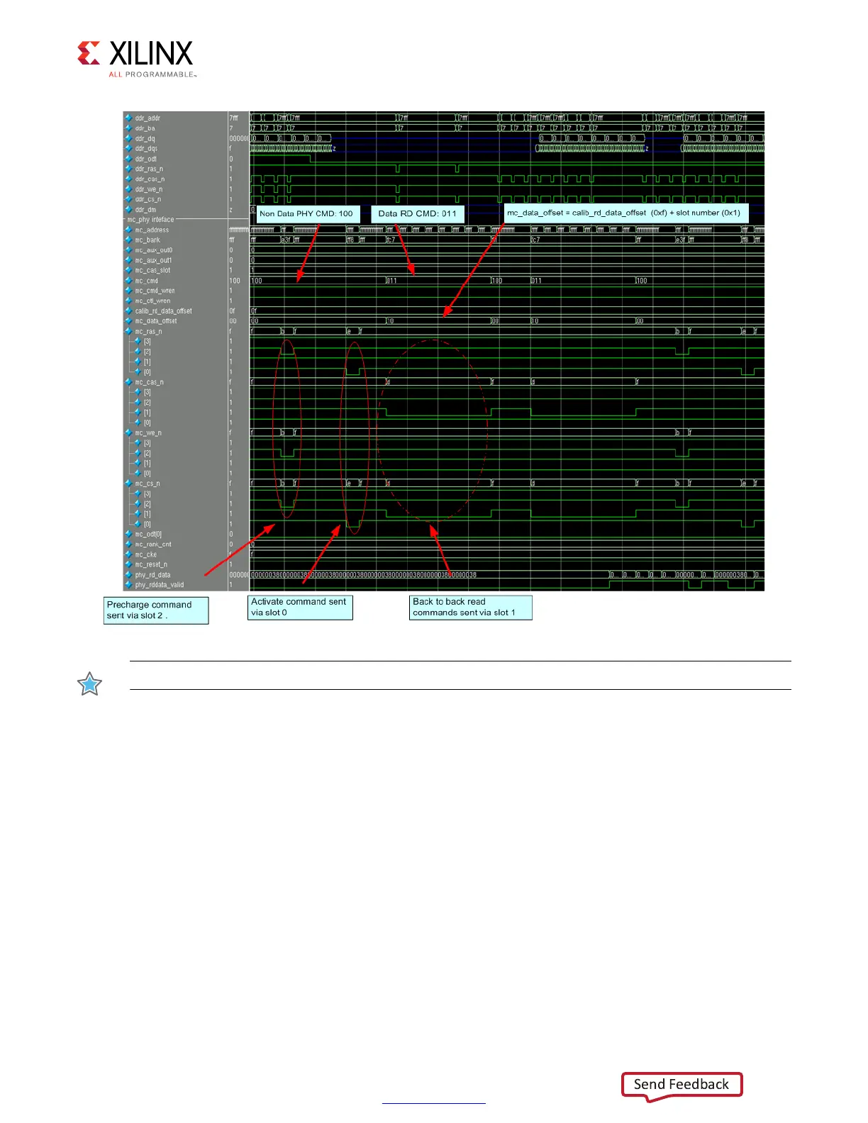
Figure 1-90: Sending Read Commands in the PHY Interface
 Loading...


