EasyManuals Logo

Xilinx Zynq-7000 User Manual

Xilinx Zynq-7000
678 pages
To Next Page IconTo Next Page
To Previous Page IconTo Previous Page
Page #178 background imageLoading...
Page #178 background image
Zynq-7000 AP SoC and 7 Series FPGAs MIS v4.1 178
UG586 November 30, 2016
www.xilinx.com
Chapter 1: DDR3 and DDR2 SDRAM Memory Interface Solution
IMPORTANT: Bits[31:27, 24:23, 14:12, and 7:3] in Table 1-58, page 136 are not used in this example.
The write waveform shown in Figure 1-90 illustrates an example with calibrated PHY read
data offset = 10. For a selected slot number of 1, nCK_PER_CLK of 4, the read data offset is:
Read data offset = Calibrated PHY read data offset + slot number
= 10 + 1 = 11
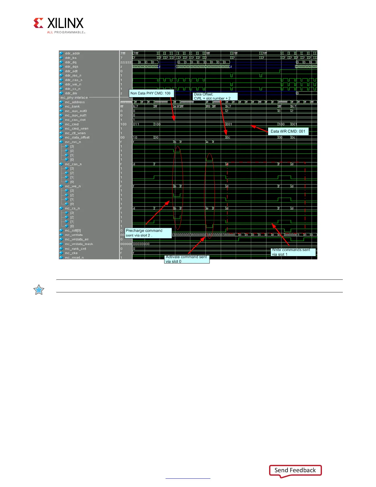
X-Ref Target - Figure 1-89
Figure 1-89: Sending Write Commands in the PHY Interface (CWL = 9)
Send Feedback

Table of Contents

Other manuals for Xilinx Zynq-7000

Questions and Answers:

Question and Answer IconNeed help?

Do you have a question about the Xilinx Zynq-7000 and is the answer not in the manual?

Xilinx Zynq-7000 Specifications

General IconGeneral
SeriesZynq-7000
Number of CoresDual-core
Processor SpeedUp to 1 GHz
Device TypeSoC
Logic CellsUp to 350K
DSP SlicesUp to 900
External Memory InterfacesDDR3, DDR2, LPDDR2
I/O StandardsLVCMOS, HSTL, SSTL
Operating Temperature-40°C to +100°C (Industrial), 0°C to +85°C (Commercial)
Package OptionsVarious BGA packages
I/O Voltage3.3V

Related product manuals