Zynq-7000 AP SoC and 7 Series FPGAs MIS v4.1 200
UG586 November 30, 2016
www.xilinx.com
Chapter 1: DDR3 and DDR2 SDRAM Memory Interface Solution
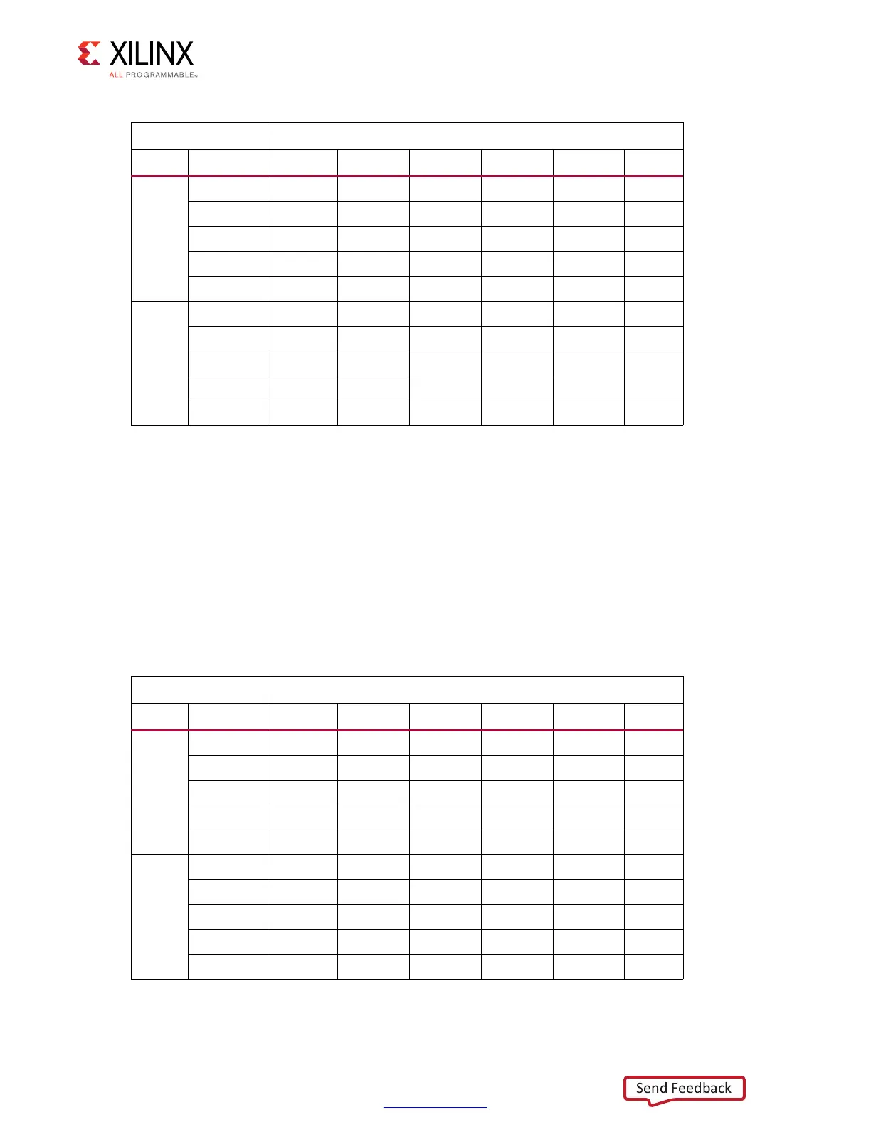
For example, if an 1,866 rated –3 FPGA operates at 1,600 Mb/s with a 1,600 rated DDR3
component, the DQ to DQS skew limit is ±31.3 ps. If the interface operates at 1,066 with a
1,333 rated DDR3 component, the skew limit is ±150 ps.
Similarly, the specified CK to address/control skew limit can be increased if the memory
interface is not operated at the maximum frequency. Table 1-68 indicates the relaxed skew
limit (±) for these cases. The vertical axis is the bit rate in Mb/s. The horizontal axis is the
DDR3 SDRAM component speed rating. The top portion of the chart is for skew changes
relative to the 1,867 Mb/s rated FPGAs, while the lower portion is for the 1,600 Mb/s rated
FPGAs.
1,066
1,866 – – – – – –
1,600 – – – – – –
1,333 – – – – – –
1,066 98.7 85.7 67.5 40.0 5.0 –
800 150.0 150.0 150.0 150.0 150.0 98.5
800
1,866 – – – – – –
1,600 – – – – – –
1,333 – – – – – –
1,066 – – – – – –
800 150.0 148.2 130.0 102.5 67.0 5.0
Table 1-68: CK to Address/Control Skew Limit
FPGA Rating Memory Component Rating
Rated Actual 2,133 1,866 1,600 1,333 1,066 800
1,866
1,866 35.0 25.0 – – – –
1,600 124.1 114.1 94.1 – – –
1,333 150.0 150.0 150.0 150.0 – –
1,066 150.0 150.0 150.0 150.0 150.0 –
800 150.0 150.0 150.0 150.0 150.0 150.0
1,600
1,866 – – – – – –
1,600 55.0 45.0 25.0 – – –
1,333 150.0 150.0 150.0 130.2 – –
1,066 150.0 150.0 150.0 150.0 150.0 –
800 150.0 150.0 150.0 150.0 150.0 150.0
Table 1-67: DQ to DQS Skew Limit (Cont’d)
FPGA Rating Memory Component Rating
Rated Actual 2,133 1,866 1,600 1,333 1,066 800
 Loading...


