Zynq-7000 AP SoC and 7 Series FPGAs MIS v4.1 215
UG586 November 30, 2016
www.xilinx.com
Chapter 1: DDR3 and DDR2 SDRAM Memory Interface Solution
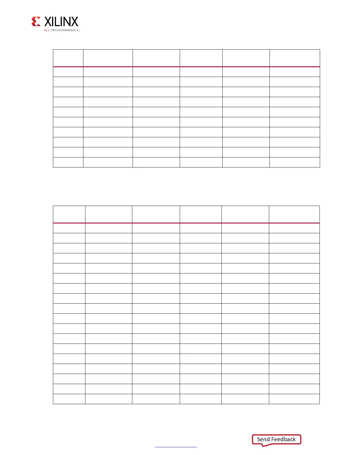
Table 1-70 shows an example of a 32-bit DDR3 interface contained within two banks. This
example uses 2 Gb x8 components.
1A8 A_08 N 9 –
1A7 A_07 P 8 DQS-P
1A6 A_06 N 7 DQS-N
1A5 A_05 P 6 –
1A4 A_04 N 5 –
1A3 A_03 P 4 –
1A2 A_02 N 3 –
1A1 A_01 P 2 –
1A0 A_00 N 1 –
1VRN – SE 0 –
Table 1-70: 32-Bit DDR3 Interface Contained in Two Banks
Bank Signal Name Byte Group I/O Type I/O Number
Special
Designation
1VRP – SE 49 –
1– D_11P 48 –
1– D_10N 47 –
1– D_09P 46 –
1– D_08N 45 –
1– D_07P 44 DQS-P
1– D_06N 43DQS-N
1– D_05P 42 –
1– D_04N 41 –
1– D_03P 40 –
1– D_02N 39 –
1– D_01P 38 –
1– D_00N 37 –
1– C_11P 36 –
1– C_10N 35 –
1– C_09P 34 –
1– C_08N 33 –
1– C_07P 32 DQS-P
Table 1-69: 16-Bit DDR3 Interface Contained in One Bank (Cont’d)
Bank Signal Name Byte Group I/O Type I/O Number
Special
Designation
 Loading...


