Zynq-7000 AP SoC and 7 Series FPGAs MIS v4.1 43
UG586 November 30, 2016
www.xilinx.com
Chapter 1: DDR3 and DDR2 SDRAM Memory Interface Solution
• DCI Cascade – This selection enables the VRN/VRP pins that are available in High
Performance banks to allocate for the address/control and reset_n ports.
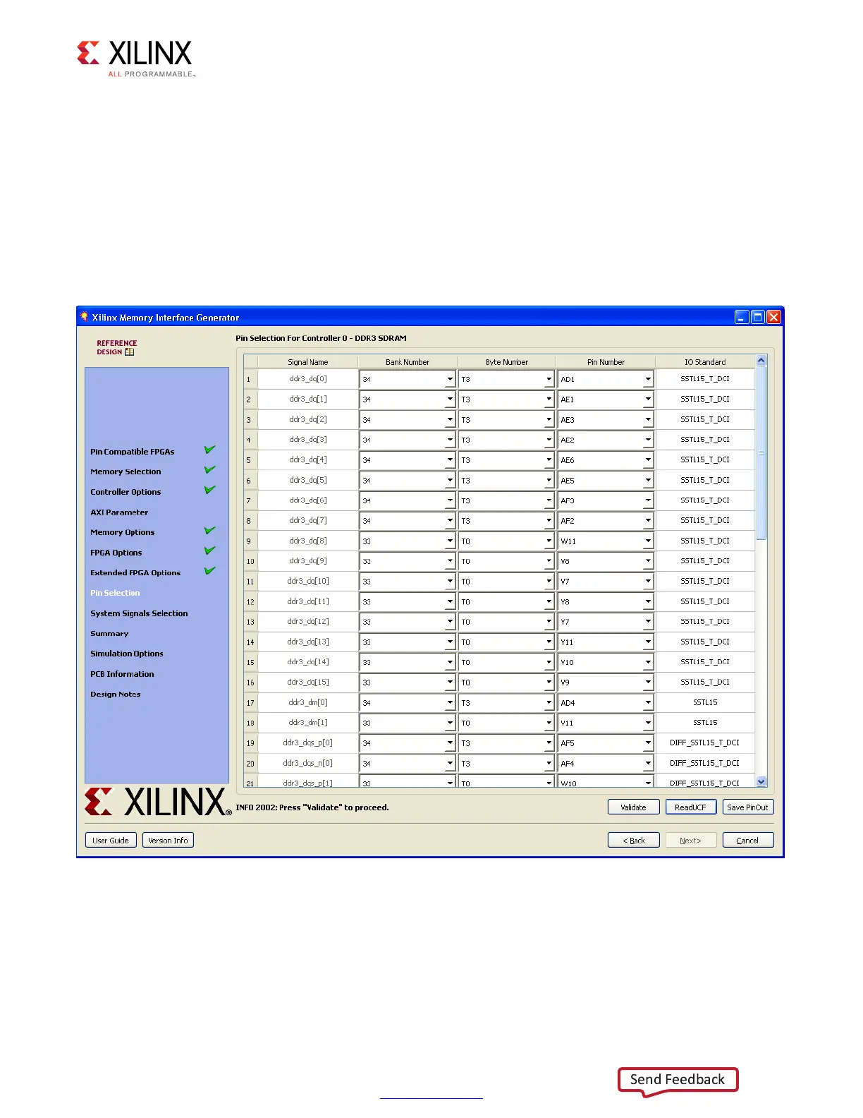
• Pin/Bank Selection Mode – This allows you to specify an existing pinout and generate
the RTL for this pinout, or pick banks for a new design. Figure 1-24 shows the options
for using an existing pinout. You must assign the appropriate pins for each signal. A
choice of each bank is available to narrow down the list of pins. It is not mandatory to
select the banks prior to selection of the pins. Click Validate to check against the MIG
pinout rules. You cannot proceed until the MIG DRC has been validated by clicking
Validate.
X-Ref Target - Figure 1-24
Figure 1-24: Pin/Bank Selection Mode
 Loading...


