Zynq-7000 AP SoC and 7 Series FPGAs MIS v4.1 45
UG586 November 30, 2016
www.xilinx.com
Chapter 1: DDR3 and DDR2 SDRAM Memory Interface Solution
For devices implemented with SSI technology, the SLRs are indicated by a number in the
header in each bank, for example, SLR 1. Interfaces cannot span across Super Logic Regions.
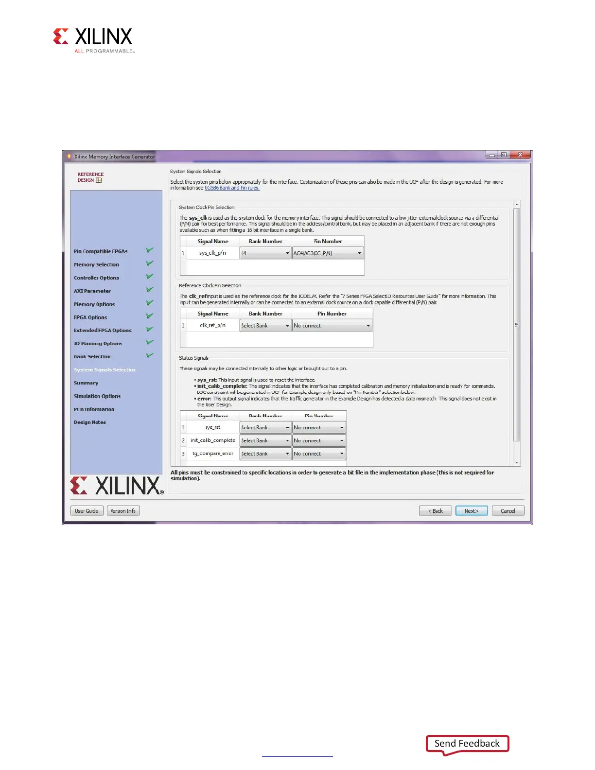
Select the pins for the system signals on this page (Figure 1-26). The MIG tool allows the
selection of either external pins or internal connections, as desired.
• sys_clk – This is the system clock input for the memory interface and is typically
connected to a low-jitter external clock source. Either a single input or a differential
pair can be selected based on the System Clock selection in the FPGA Options page
(Figure 1-22). The sys_clk input must be in the same column as the memory
interface. If this pin is connected in the same banks as the memory interface, the MIG
tool selects an I/O standard compatible with the interface, such as DIFF_SSTL15 or
SSTL15. If sys_clk is not connected in a memory interface bank, the MIG tool selects
an appropriate standard such as LVCMOS18 or LVDS. The XDC can be modified as
desired after generation.
X-Ref Target - Figure 1-26
Figure 1-26: System Pins
 Loading...


