Zynq-7000 AP SoC and 7 Series FPGAs MIS v4.1 454
UG586 November 30, 2016
www.xilinx.com
Chapter 3: RLDRAM II and RLDRAM 3 Memory Interface Solutions
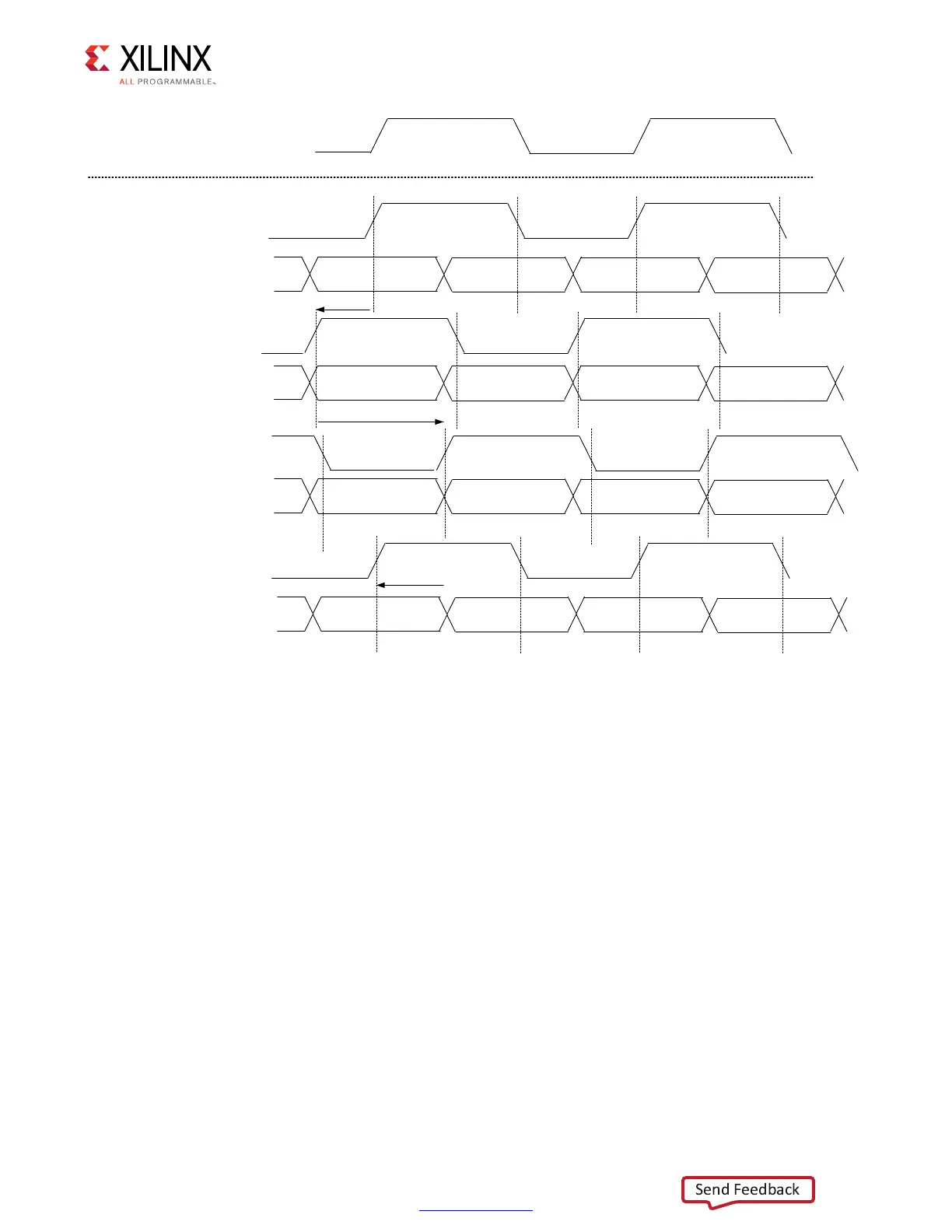
Figure 3-56 shows the second stage of RLDRAM II write calibration for in which the entire
byte lane is shifted in relation to the CK to sweep and find where the write data transfer
breaks for the DK-to-CK alignment.
X-Ref Target - Figure 3-55
Figure 3-55: RLDRAM II Write Calibration (Stage 1, DK-to-DQ)
“Ideal”, starting
point. Also just
used in Sim.
A/C Bank
CK
0 taps
Starting point
for sweep of
DK clock
Byte lane
with a DK
Right edge
found
DK
Stage 1 (PHASER_OUT stage 3)
Rise
DQ
Fall
Rise
Fall
(1)
(2)
(3)
DK
Rise
DQ
Fall
Rise
Fall
DK
Rise
DQ
Fall
Rise
Fall
Final Spot for
the DK clock
Rise
DQ
Fall
Rise
Fall
(4)
DK
DK Shift
DK Shift
DK Shift
 Loading...


