Zynq-7000 AP SoC and 7 Series FPGAs MIS v4.1 455
UG586 November 30, 2016
www.xilinx.com
Chapter 3: RLDRAM II and RLDRAM 3 Memory Interface Solutions
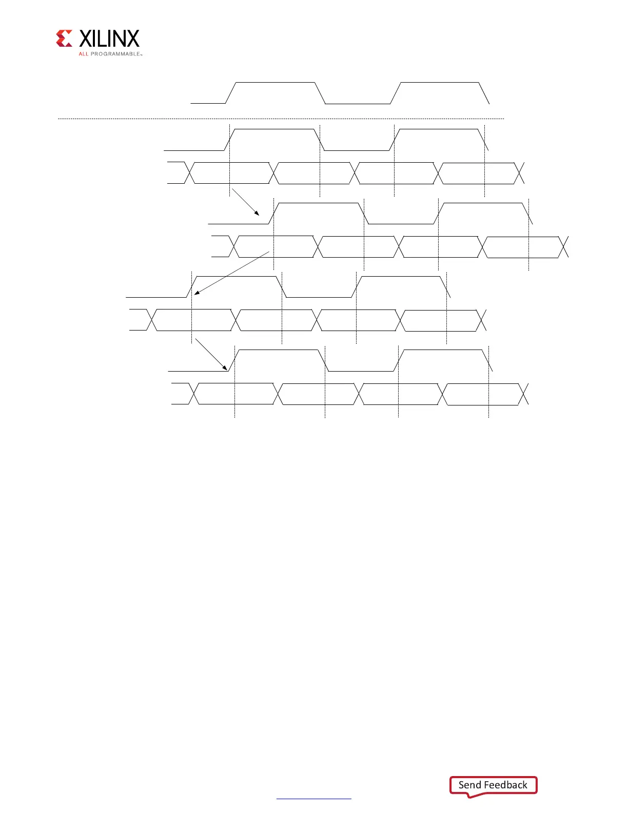
Figure 3-57 shows the last step of RLDRAM II write calibration, where the byte lanes that do
not share a DK clock as part of their PHASER_OUT output, are calibrated with respect to the
DK clock in another byte lane.
X-Ref Target - Figure 3-56
Figure 3-56: RLDRAM II Write Calibration (Stage 2, DK-to-CK)
Rise
DQ
Fall
Rise
Fall
(1)
DK
Rise
DQ
Fall
Rise
Fall
(2)
DK
Rise
DQ
Fall
Rise
Fall
(3)
DK
Rise
DQ
Fall
Rise
Fall
(4)
DK
Sweep to the
right until
failure or end
of taps
Starting point
Sweep to the
left until
failure or hit 0
taps
Final Point
A/C Bank
CK
 Loading...


