Zynq-7000 AP SoC and 7 Series FPGAs MIS v4.1 606
UG586 November 30, 2016
www.xilinx.com
Chapter 4: LPDDR2 SDRAM Memory Interface Solution
In the third scenario, because operating in frequencies < 400 MHz and PHASER_IN is
operating in DIV2 mode, you would not be able to find the right noise region with 64 taps.
Thus, assume that you are close to left noise region and bring back the PHASER_IN fine taps
values to their initial position. After the PHASER_IN fine taps increments/decrements, use
IDELAY taps to delay the DQ to find both the edges (third case). When both edges are
detected, the final DQS tap value is computed as:
first_edge_taps + (second_edge_taps – first_edge_taps)/2.
When only one edge is detected, the final DQS tap value is computed as:
(first_edge_taps + (31 – first_edge_taps)/2)
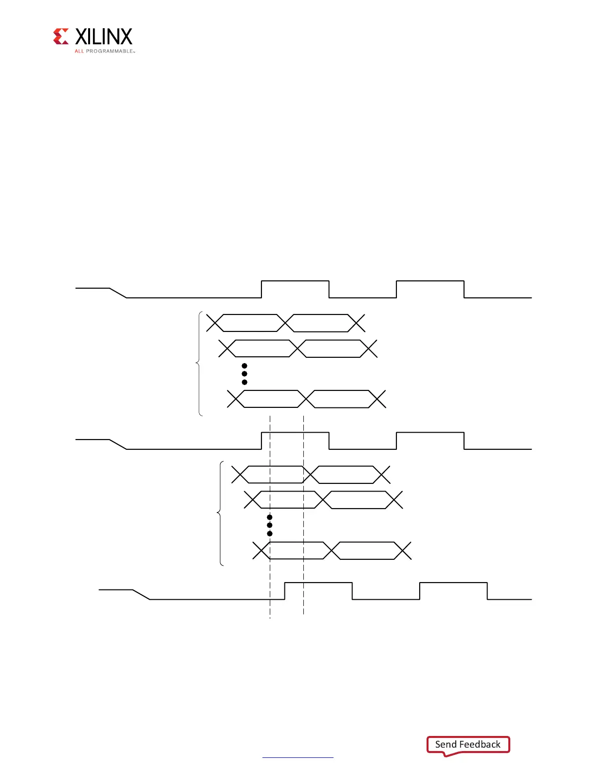
Figure 4-53 shows the timing diagram for DQS center alignment in the data valid window.
X-Ref Target - Figure 4-53
Figure 4-53: Read Leveling Stage 1 Timing Diagram
)NITIAL$13
)NITIAL$1"ITS
$1"ITS$ELAYEDUSING
)$%,!94APS
8
$13AT,EFT7INDOW%DGE
$13#ENTEREDIN6ALID
7INDOW
 Loading...


