Zynq-7000 AP SoC and 7 Series FPGAs MIS v4.1 493
UG586 November 30, 2016
www.xilinx.com
Chapter 3: RLDRAM II and RLDRAM 3 Memory Interface Solutions
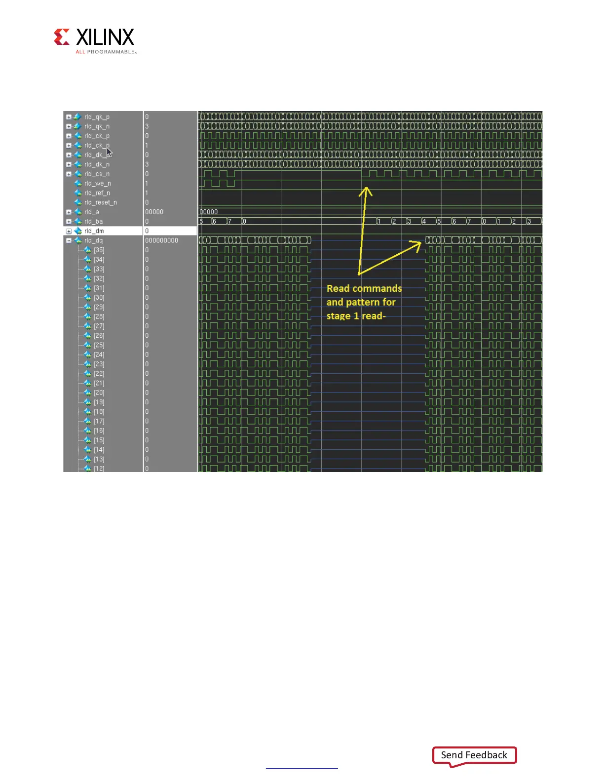
This pattern is then continuously read back while the calibration is completed, as shown in
Figure 3-70.
The second stage performs an alignment to ensure data is returned in the correct order. The
length of the data pattern depends on the ratio of the memory clock to the FPGA logic
clock. For RLDRAM II, the data pattern of A_5_0_F is first written to the memory and
continuously read back and adjusted internally if required.
For RLDRAM 3, the data pattern of A_5_0_F_9_6_D_2 is first written to the memory and
continuously read back and adjusted internally if required.
The third stage performs a read enable calibration. The data pattern used during this stage
is the same pattern used during the second stage of calibration. The data pattern is first
written to the memory, and then read back for the read enable calibration, as shown in
Figure 3-71.
X-Ref Target - Figure 3-70
Figure 3-70: Reads for First Stage Read Calibration
 Loading...


