Zynq-7000 AP SoC and 7 Series FPGAs MIS v4.1 597
UG586 November 30, 2016
www.xilinx.com
Chapter 4: LPDDR2 SDRAM Memory Interface Solution
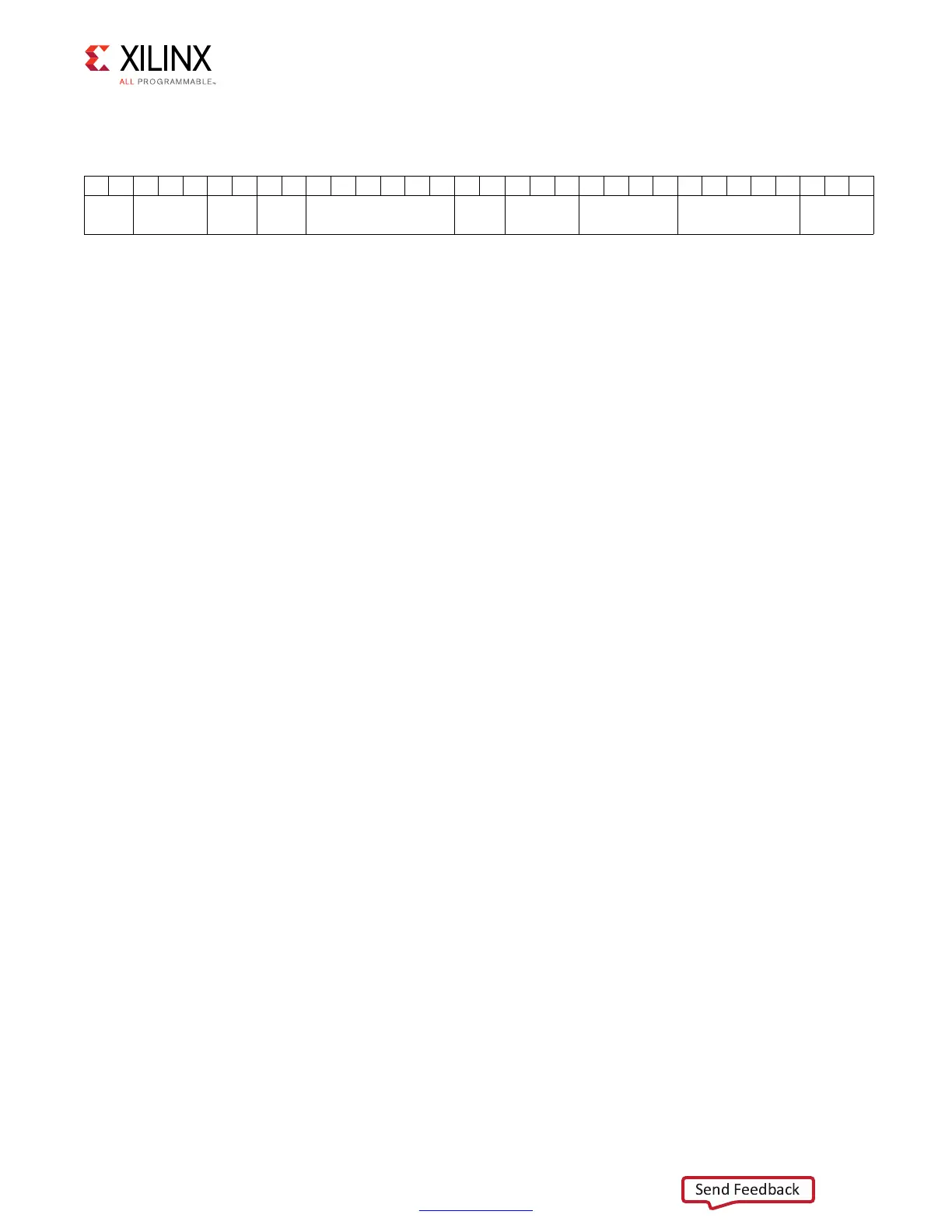
The PHY control word is broken down into several fields, as shown in Table 4-22.
• PHY Command – This field defines the actions undertaken by the PHY control block to
manage command and data flow through the dedicated PHY. The PHY commands are:
°
Write (Wr – 0x01) – This command instructs the PHY control block to read the
address, command, and data OUT_FIFOs and transfer the data read from those
FIFOs to their associated IOIs.
°
Read (Rd – 0x03) – This command instructs the PHY control block to read the
address, command OUT_FIFOs, and transfer the data read from those FIFOs to their
associated IOIs. In addition, data read from the memory is transferred after its
arrival from the data IOIs to the Data IN_FIFO.
°
Non-Data (ND – 0x04) – This command instructs the PHY control block to read the
address and command OUT_FIFOs and transfer the data read from those FIFOs to
their associated IOIs.
• Control Offset – This field is used to control when the address and command
IN/OUT_FIFOs are read and transferred to the IOIs. The control offset is in units of the
LPDDR2 SDRAM clock cycle.
• Auxiliary Output – This field is used to control when the auxiliary output signals
(Aux_Output[3:0]) are used. Auxiliary outputs can be configured to activate during
read and write commands. The timing offset and duration are controlled by the
attributes described in Table 4-23, page 598. These outputs are not used by the
LPDDR2 interface generated by the MIG tool; they are set to 0.
• Low Index (Bank) – The dedicated PHY has internal counters that require this field to
specify which of the eight LPDDR2 SDRAM banks to use for the data command. The
MIG IP core does not use these internal counters; therefore, this field should be all
zeros.
• Reserved – This field must always be set to 2'b00.
• Data Offset – This field is used to control when the data IN/OUT_FIFOs are read or
written based on the PHY command. The data offset is in units of the LPDDR2 SDRAM
clock cycle.
• Seq – This field contains a sequence number used in combination with the Sync_In
control signal from the PLL to keep two or more PHY control blocks executing the
commands read from their respective control queues in sync. Commands with a given
seq value must be executed by the command parser within the PHY control block
during the specific phase indicated by the Seq field.
• CAS Slot – The slot number being used by the Memory Controller for write/read (CAS)
commands.
Table 4-22: PHY Control Word
31 30 29 28 27 26 25 24 23 22 21 20 19 18 17 16 15 14 13 12 11 10 9 8 7 6 5 4 3 2 1 0
Act
Pre
Event
Delay
CAS
Slot
Seq Data Offset Reser
ved
Low
Index
Aux_Out Control Offset PHY Cmd
 Loading...


