Zynq-7000 AP SoC and 7 Series FPGAs MIS v4.1 81
UG586 November 30, 2016
www.xilinx.com
Chapter 1: DDR3 and DDR2 SDRAM Memory Interface Solution
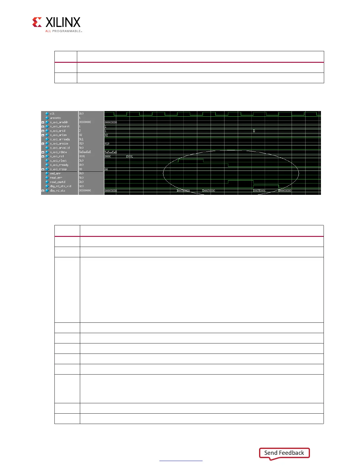
The status generated for a read transaction is shown in Figure 1-45.
5:2 Response ID for the write response
1:0 Write response received for AXI
Table 1-15: Debug Status for the Write Transaction (Cont’d)
Bits Description
X-Ref Target - Figure 1-45
Figure 1-45: Status for the Read Transaction
Table 1-16: Debug Status for the Read Transaction
Bits Description
39:32 Number of beats/read transfers completed for last burst
31:30 Reserved
29:27
Data pattern used for the current check:
• 000: 5A and A5
• 001: PRBS pattern
• 010: Walking zeros
• 011: Walking ones
• 100: All ones
• 101: All zeros
26:19 Pointer value for which the mismatch occurred
18 Data mismatch occurred between the written data and read data
17 Read error occurred, read transaction could not be completed
16 Command error occurred during read transaction
15:4 Reserved
3:2
AXI wrapper read FSM state when timeout (watchdog timer should be enabled) occurs:
• 2'b01: Read command transaction
• 2'b10: Data read transaction
1 Incorrect response ID presented by the AXI slave
0 Read error response on AXI
 Loading...


