Zynq-7000 AP SoC and 7 Series FPGAs MIS v4.1 80
UG586 November 30, 2016
www.xilinx.com
Chapter 1: DDR3 and DDR2 SDRAM Memory Interface Solution
The initialization and the calibration sequence remain the same as that indicated in
Simulating the Example Design (for Designs with the Standard User Interface), page 66. The
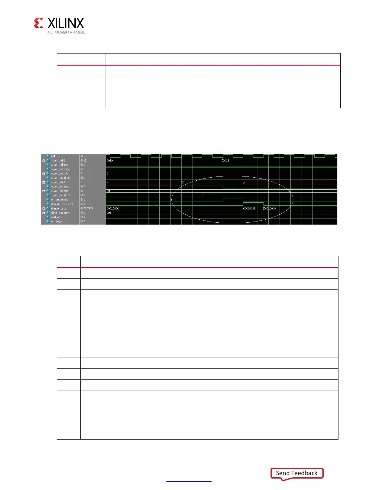
status that is generated for a write transaction can be found in Figure 1-44.
dbg_rd_sts_vld
When asserted, this signal indicates a valid status for the read transaction on the
dbg_rd_sts bus. This signal is asserted even if the read transaction does not
complete.
dbg_rd_sts
This signal has the status of the read transaction. The details of the status are given
in Table 1-16.
Table 1-14: Signals of Interest During Simulation for the AXI4 Test Bench
Signal Description
X-Ref Target - Figure 1-44
Figure 1-44: Status for the Write Transaction
Table 1-15: Debug Status for the Write Transaction
Bits Description
39:32 Number of beats/write transfers completed for last burst
31:21 Reserved
20:18
Data pattern used for the current transaction:
• 000: 5A and A5
• 001: PRBS pattern
• 010: Walking zeros
• 011: Walking ones
• 100: All ones
• 101: All zeros
17 Write error occurred. The write transaction could not be completed.
16 Command error occurred during a write transaction.
15:9 Reserved
8:6
AXI wrapper write FSM state when timeout (watchdog timer should be enabled) occurs:
• 3'b001: Data write transaction
• 3'b010: Waiting for acknowledgment for written data
• 3'b011: Dummy data write transaction
• 3'b100: Waiting for response from the response channel
 Loading...


