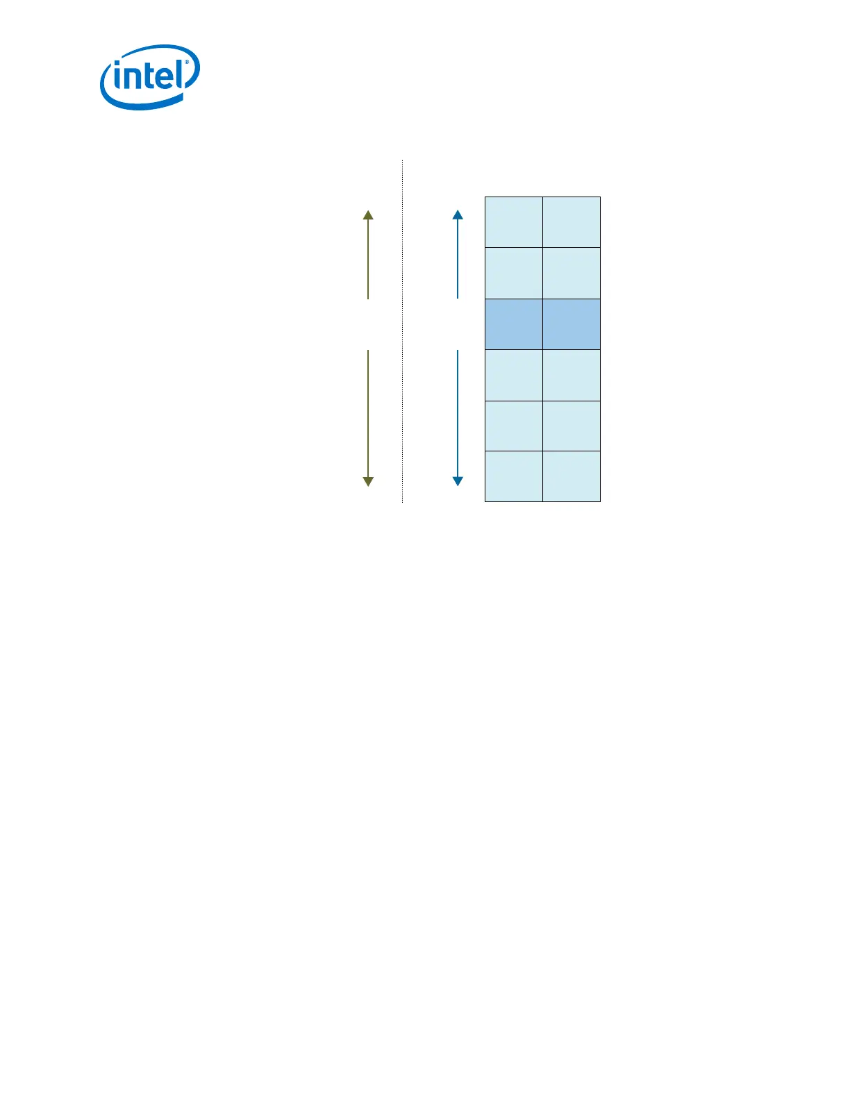
Figure 185. PMA and PCS Bonding
Slave PCS
Channel
PMA
Slave PCS
Channel
PMA
Master PCS
Channel
PMA
Slave PCS
Channel
PMA
Slave PCS
Channel
PMA
Slave PCS
Channel
PMA
Distribution
Delay (Cycles)
4
2
0
2
4
6
Starting
Delay (Cycles)
2
4
6
4
2
0
For PMA and PCS bonding, the concept of master and slave channels is used. One PCS
channel in the bonded group is selected as the master channel and all others are slave
channels. To ensure that all channels start transmitting data at the same time and in
the same state, the master channel generates a start condition. This condition is
transmitted to all slave channels. The signal distribution of this start condition incurs a
two parallel clock cycle delay. Because this signal travels sequentially through each
PCS channel, this delay is added per channel. The start condition used by each slave
channel is delay compensated based on the slave channel's distance from the master
channel. This results in all channels starting on the same clock cycle.
The transceiver PHY IP automatically selects the center channel to be the master PCS
channel. This minimizes the total starting delay for the bonded group. For PLL
feedback compensation bonding up to all channels on one side can be bonded if the
master PCS channel is placed in the center of the bonded group.
Note: Because the PMA and PCS bonding signals travel through each PCS block, the PMA and
PCS bonded groups must be contiguously placed. The channel order needs to be
maintained when doing the pin assignments to the dedicated RX serial inputs and TX
serial outputs (for example: PIN_BC7 and PIN_BC8 for GXBR4D_TX_CH0p and
GXBR4D_TX_CH0n TX serial outputs). Channels need to be placed in an ascending
order from bottom to top. Swapping of channels, when doing pin assignments, leads
to errors.
3.9.3. Selecting Channel Bonding Schemes
In Arria 10 devices, select PMA and PCS bonding for bonded protocols that are
explicitly supported by the hard PCS blocks. For example, PCI Express, SFI-S, and
40GBASE-KR.
3. PLLs and Clock Networks
UG-01143 | 2018.06.15
Intel
®
Arria
®
10 Transceiver PHY User Guide
392