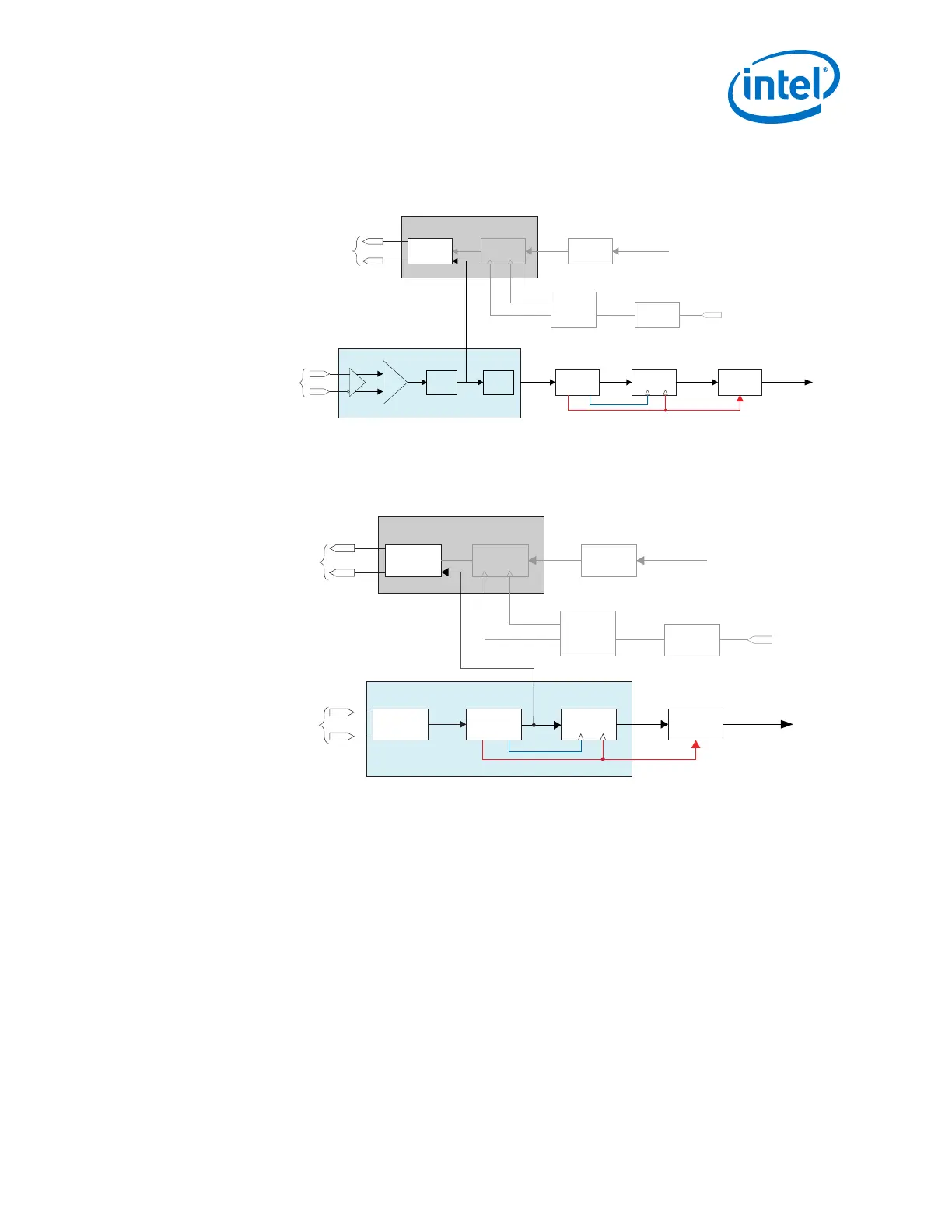
Figure 234. Reverse Serial Loopback Path/Pre CDR
The reverse serial loopback path sets the transmitter buffer to transmit data fed directly from the VGA output.
Adjusting the RX CTLE, and RX VGA settings has an effect on the serial data that goes through the diagnostic
loopback path.
Transmitter
PCS
Serializer
Transmitter
Buffer
Transmitter
PLL
Parallel Data
from FPGA Core
Parallel
Data
Serial
Data
Serial
Clock
Input
Reference
Clock
Transmitter PMA
Clock
Generation
Block
Parallel
Clock
Receiver
PCS
Deserializer
Parallel Data
to FPGA Core
Parallel
Data
Serial
Data
Receiver Buffer
CDR
Serial
Data
Transmitter Serial
Differential Output
Data
Receiver Serial
Differential Input
Data
Serial Clock
Parallel Clock
Diagnostic
Loopback
CTLE
VGA DFE
Figure 235. Reverse Serial Loopback Path/Post CDR
The reverse serial loopback path sets the transmitter buffer to transmit data fed directly from the CDR
recovered data. Adjusting the RX CTLE, RX VGA, and RX DFE settings has an effect on the serial data that goes
through the reverse loopback path. Adjusting TX VOD and TX pre-emphasis has an effect on the transmitter
serial differential output data.
Transmitter
Buffer
Serial
Data
Transmitter Serial
Differential Output
Data
Transmitter PMA
Receiver
PCS
Deserializer
Parallel Data
to FPGA core
Parallel
Data
Serial
Data
Receiver PMA
CDR
Serial
Data
Receiver
Buffer
Transmitter
PCS
Serializer
Transmitter
PLL
Parallel Data
Parallel
Data
Serial
Clock
Input
Reference
Clock
Clock
Generation
Block
Parallel
Clock
Receiver Serial
Differential Input
Data
Reverse
Loopback
Serial Clock
Parallel Clock
from FPGA core
5.2. Arria 10 Enhanced PCS Architecture
You can use the Enhanced PCS to implement multiple protocols that operate at around
10 Gbps or higher line rates.
The Enhanced PCS provides the following functions:
• Performs functions common to most serial data industry standards, such as word
alignment, block synchronization, encoding/decoding, and framing, before data is
sent or received off-chip through the PMA
• Handles data transfer to and from the FPGA fabric
• Internally handles data transfer to and from the PMA
• Provides frequency compensation
• Performs channel bonding for multi-channel low skew applications
5. Arria 10 Transceiver PHY Architecture
UG-01143 | 2018.06.15
Intel
®
Arria
®
10 Transceiver PHY User Guide
461