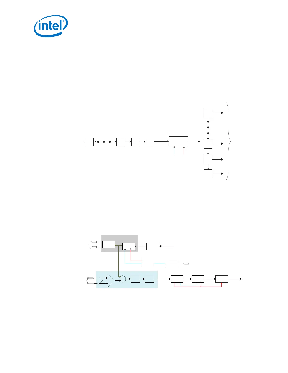
5.1.2.3. Deserializer
The deserializer block clocks in serial input data from the receiver buffer using the
high-speed serial recovered clock and deserializes the data using the low-speed
parallel recovered clock. The deserializer forwards the deserialized data to the receiver
PCS or FPGA fabric, and sends out the LSB of the input data first.
The deserializer supports the following deserialization factors: 8, 10, 16, 20, 32, 40,
and 64.
Figure 232. Deserializer Block Diagram
Dn D2 D1 D0
Serial
Data
LSB
Deserializer
Parallel
Clock
Clock
Serial
Dn
D2
D1
D0
Parallel
Data
5.1.3. Loopback
The PMA supports serial, diagnostic, and reverse loopback paths.
Figure 233. Serial Loopback Path
The serial loopback path sets the CDR to recover the data from the serializer while data from receiver serial
input pin is ignored by the CDR. The transmitter buffer sends data normally. Adjusting the TX VOD, TX pre-
emphasis, and RX CTLE settings does not have an effect on the serial data that goes through the serial
loopback path. Adjusting the RX VGA and RX DFE settings has an effect on the serial data that goes through
the serial loopback path.
Transmitter
Buffer
Serial
Data
Transmitter PMA
Receiver Buffer
Serial
Loopback
Receiver Serial
Differential Input
Data
Transmitter Serial
Differential Output
Data
Transmitter
PCS
Serializer
Transmitter
PLL
Parallel Data
Parallel
from FPGA Core
Data
Serial
Clock
Input
Reference
Clock
Clock
Generation
Block
Parallel
Clock
Receiver
PCS
Deserializer
Parallel Data
to FPGA Core
Parallel
Data
Serial
Data
Serial Clock
CDR
Serial
Data
Parallel Clock
CTLE
VGA DFE
5. Arria 10 Transceiver PHY Architecture
UG-01143 | 2018.06.15
Intel
®
Arria
®
10 Transceiver PHY User Guide
460