• Avalon Interface Specifications
The ports related to reconfiguration are compliant with the Avalon
Specification. Refer to the Avalon Specification for more details about these
ports.
• Intel Arria 10 device fPLL reports an unlocked condition
3.1.4. CMU PLL
The clock multiplier unit (CMU) PLL resides locally within each transceiver channel.The
channel PLL's primary function is to recover the receiver clock and data in the
transceiver channel. In this case the PLL is used in clock and data recovery (CDR)
mode.
When the channel PLL of channels 1 or 4 is configured in the CMU mode, the channel
PLL can drive the local clock generation block (CGB) of its own channel, then the
channel cannot be used as a receiver.
The CMU PLL from transceiver channel 1 and channel 4 can also be used to drive other
transceiver channels within the same transceiver bank. The CDR of channels 0, 2, 3,
and 5 cannot be configured as a CMU PLL.
For datarates lower than 6 Gbps, the local CGB divider has to be engaged (TX local
division factor in transceiver PHY IP under the TX PMA tab) .
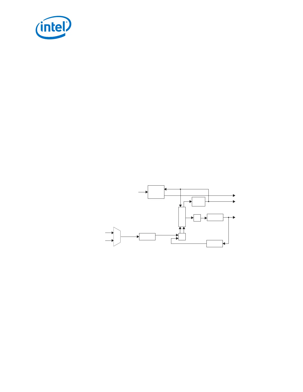
Figure 172. CMU PLL Block Diagram
VCO
PFD
CP &
LF
M Counter
N Counter
L Counter
Lock to
Reference
Controller
User Control
(LTR/LTD)
Lock to Reference
PLL Lock Status
Output
Lock
Detector
Reference clock network
Up
Down
Input reference
clock
refclk
fbclk
Receiver input pin
Refclk
Multiplexer
Input Reference Clock
The input reference clock for a CMU PLL can be sourced from either the reference
clock network or a receiver input pin. The input reference clock is a differential signal.
For protocol jitter compliance at data rates > 10 Gbps, Intel recommends using the
dedicated reference clock pin in the same triplet with the CMU PLL as the input
reference clock source.The input reference clock must be stable and free-running at
device power-up for proper PLL operation. If the reference clock is not available at
device power-up, then you must recalibrate the PLL when the reference clock is
available. Refer to the Calibration section for details about PLL calibration and the
CLKUSR clock requirement.
Note:
The CMU PLL calibration is clocked by the CLKUSR clock which must be stable and
available for calibration to proceed. Refer to the Calibration section for more details
about the CLKUSR clock.
Reference Clock Multiplexer (Refclk Mux)
3. PLLs and Clock Networks
UG-01143 | 2018.06.15
Intel
®
Arria
®
10 Transceiver PHY User Guide
368