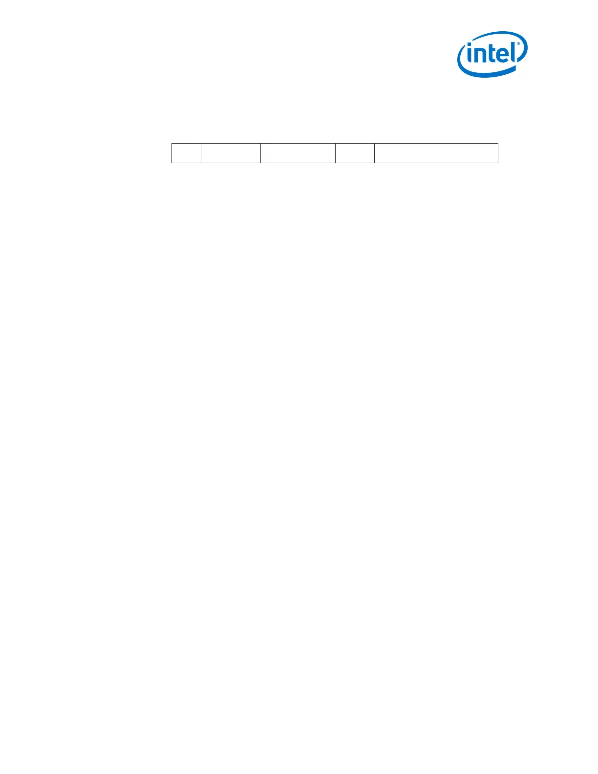
The tx_enh_frame_diag_status[1:0] input from the FPGA fabric is inserted into
the Status field each time a DIAG word is created by the framing generator.
Figure 31. Interlaken Diagnostic Word
bx10 b011001
66 63 58
h000000
57 33
Status
32 31
CRC32
034
2.5.2. Interlaken Configuration Clocking and Bonding
The Arria 10 Interlaken PHY layer solution is scalable and has flexible data rates. You
can implement a single lane link or bond up to 48 lanes together. You can choose a
lane data rate up to 17.4 Gbps for GX devices and 25.8 Gbps for GT devices. You can
also choose between different reference clock frequencies, depending on the PLL used
to clock the transceiver. Refer to the Arria 10 Device Datasheet for the minimum and
maximum data rates that Arria 10 transceivers can support at different speed grades.
You can use an ATX PLL or fPLL to provide the clock for the transmit channel. An ATX
PLL has better jitter performance compared to an fPLL. You can use the CMU PLL to
clock only the non-bonded Interlaken transmit channels. However, if you use the CMU
PLL, you lose one RX transceiver channel.
For the multi-lane Interlaken interface, TX channels are usually bonded together to
minimize the transmit skew between all bonded channels. Currently, xN bonding and
PLL feedback compensation bonding schemes are available to support a multi-lane
Interlaken implementation. If the system tolerates higher channel-to-channel skew,
you can choose to not bond the TX channels.
To implement bonded multi-channel Interlaken, all channels must be placed
contiguously. The channels may all be placed in one bank (if not greater than six
lanes) or they may span several banks.
Related Information
• Using PLLs and Clock Networks on page 398
For more information about implementing PLLs and clocks
• Arria 10 Device Datasheet
2.5.2.1. xN Clock Bonding Scenario
The following figure shows a xN bonding example supporting 10 lanes. Each lane is
running at 12.5 Gbps. The first six TX channels reside in one transceiver bank and the
other four TX channels reside in the adjacent transceiver bank. The ATX PLL provides
the serial clock to the master CGB. The CGB then provides parallel and serial clocks to
all of the TX channels inside the same bank and other banks through the xN clock
network.
Because of xN clock network skew, the maximum achievable data rate decreases
when TX channels span several transceiver banks.
2. Implementing Protocols in Arria 10 Transceivers
UG-01143 | 2018.06.15
Intel
®
Arria
®
10 Transceiver PHY User Guide
97