5.1.1.2.3. Programmable Pre-Emphasis
Pre-emphasis can maximize the eye at the far-end receiver. The programmable pre-
emphasis module in each transmit buffer amplifies high frequencies in the transmit
data signal, to compensate for attenuation in the transmission media.
The pre-tap pre-emphasizes the bit before the transition and de-emphasizes the
remaining bits. A different polarity on pre-tap does the opposite.
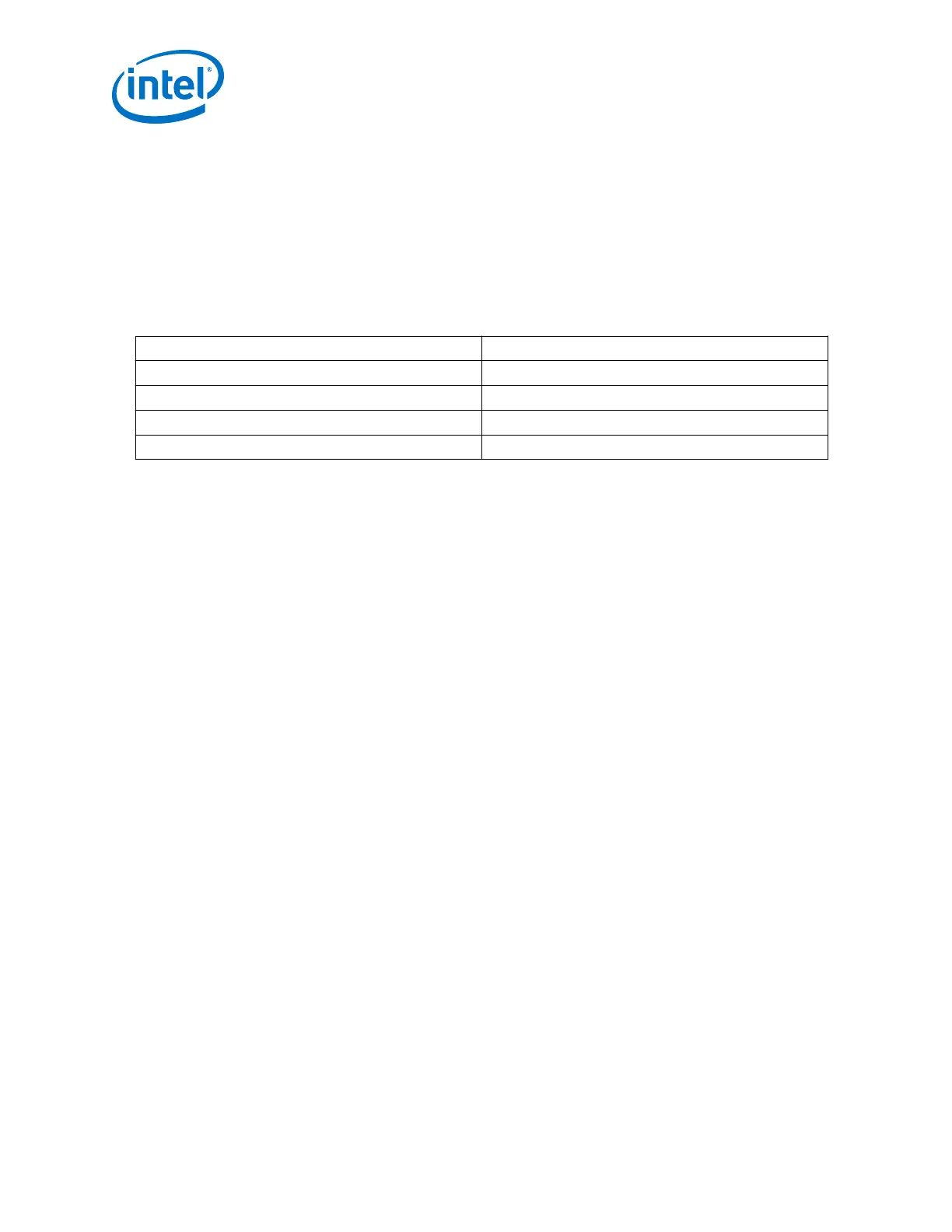
Table 251. Pre-Emphasis Taps
All four pre-emphasis taps provide inversion control, shown by negative values.
Pre-Emphasis Tap Number of Settings
Second pre-tap 15
First pre-tap 33
First post-tap 51
Second post-tap 25
You can set pre-emphasis taps through the Quartus Assignment Editor, the Avalon-MM
registers, and the QSF settings.
Related Information
For more information, refer to Arria 10 Pre-Emphasis and Output Swing Settings
5.1.1.2.4. Power Distribution Network (PDN) induced Inter-Symbol Interference (ISI)
compensation
Arria 10 Transmitter driver includes a compensation circuitry to reduce PDN induced
ISI jitter. You can enable this compensation circuitry to reduce jitter through QSF
setting, Quartus Assignment Editor or Avalon-MM interface. The power consumption
increases when you enable the compensation.
5.1.1.2.5. Programmable Transmitter On-Chip Termination (OCT)
Transmitter buffers include programmable on-chip differential termination of 85Ω,
100Ω, or OFF. You can set the OCT value through the Quartus Assignment Editor and
the Avalon-MM registers.
Related Information
Arria 10 Register Map
5.1.2. Receiver
The receiver deserializes the high-speed serial data, creates a parallel data stream for
either the receiver PCS or the FPGA fabric, and recovers the clock information from
the received data.
The receiver portion of the PMA is comprised of the receiver buffer, the clock data
recovery (CDR) unit, and the deserializer.
5. Arria 10 Transceiver PHY Architecture
UG-01143 | 2018.06.15
Intel
®
Arria
®
10 Transceiver PHY User Guide
450