If the tx_clkout that is forwarded to the FPGA fabric is used to clock the write side
of the phase compensation FIFO, then both sides of the FIFO have 0 ppm frequency
difference because it is the same clock that is used.
If you use a different clock than the tx_clkout to clock the write side of the phase
compensation FIFO, then you must ensure that the clock provided has a 0 ppm
frequency difference with respect to the tx_clkout.
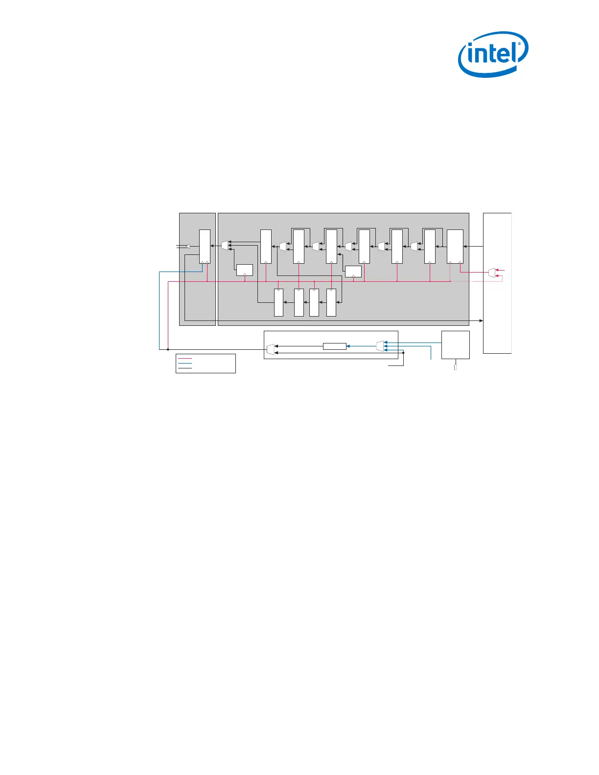
Figure 182. Transmitter Enhanced PCS and PMA Clocking
The master or local CGB provides the serial clock to the serializer of the transmitter PMA, and the parallel clock
to the transmitter PCS.
Transmitter Enhanced PCSTransmitter PMA
TX
Gearbox
tx_serial_data
Serializer
Interlaken
Disparity Generator
Scrambler
Parallel Clock
PRBS
Generator
PRP
Generator
Parallel Clock
Serial Clock
Parallel and Serial Clocks
Clock Divider
Parallel and Serial Clocks
Clock Generation Block (CGB)
Serial Clock
Input Reference Clock
ATX PLL
fPLL
CMU PLL
tx_pma_div_clkout
Enhanced PCS
TX FIFO
Interlaken
Frame Generator
Interlaken
CRC32 Generator
64B/66B Encoder
and TX SM
TX
Data &
Control
FPGA
Fabric
tx_coreclkin
tx_clkout
KR FEC
TX Gearbox
KR FEC
Scrambler
KR FEC
Encoder
Transcode
Encoder
In the Enhanced PCS, the parallel clock is used by all the blocks up to the read side of
the TX phase compensation FIFO. The clocks of all channels in bonded configuration
are forwarded. You can pick tx_clkout[0] as the source for clocking their TX logic in
core.
For the enhanced PCS, the transmitter PCS forwards the following clocks to the FPGA
fabric:
tx_clkout for each transmitter channel in non-bonded and bonded configuration. In
bonded configuration, any tx_clkout can be used depending on your core timing
requirements.
You can clock the transmitter datapath interface using one of the following methods:
• Quartus Prime selected transmitter datapath interface clock
• User-selected transmitter datapath interface clock
3.7. Receiver Data Path Interface Clocking
The CDR block present in the PMA of each channel recovers the serial clock from the
incoming data. The CDR block also divides the recovered serial clock to generate the
recovered parallel clock. Both the recovered serial and the recovered parallel clocks
are used by the deserializer. The receiver PCS can use the following clocks based on
the configuration of the receiver channel:
• Recovered parallel clock from the CDR in the PMA.
• Parallel clock from the clock divider used by the transmitter PCS (if enabled) for
that channel.
3. PLLs and Clock Networks
UG-01143 | 2018.06.15
Intel
®
Arria
®
10 Transceiver PHY User Guide
387