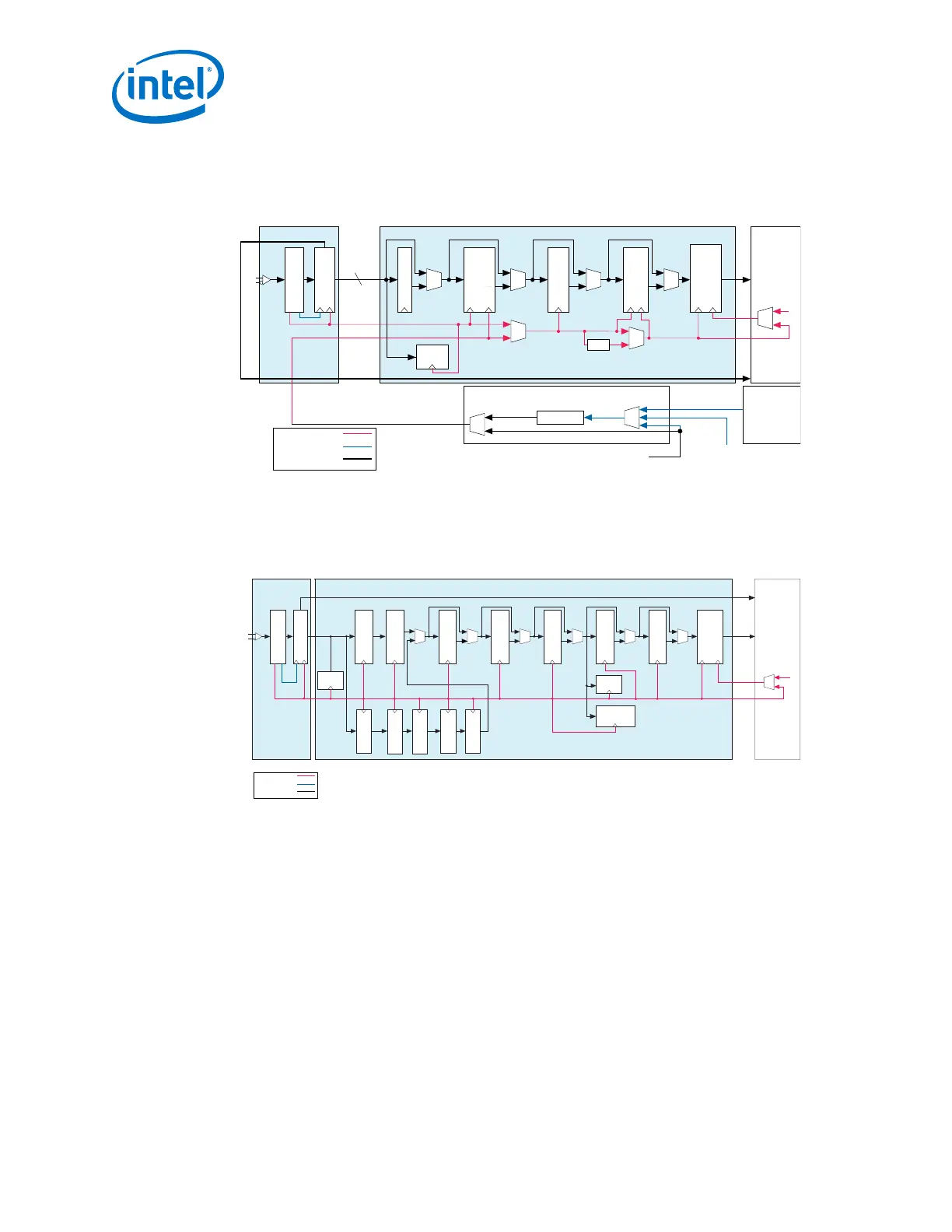
For configurations that use the byte deserializer block, the clock divided by 2 or 4 is
used by the byte deserializer and the write side of the RX phase compensation FIFO.
Figure 183. Receiver Standard PCS and PMA Clocking
RX
FIFO
Byte
Deserializer
8B/10B Decoder
Rate Match FIFO
Receiver PMA
Word Aligner
Deserializer
CDR
Receiver Standard PCS
rx_serial_data
FPGA
Fabric
/2, /4
Parallel Clock
Serial Clock
Parallel and Serial Clock Parallel and Serial Clock
Clock Divider
rx_pma_div_clkout
Serial Clock
Clock Generation Block (CGB)
ATX PLL
CMU PLL
fPLL
rx_coreclkin
rx_clkout or
tx_clkout
Parallel Clock
(Recovered)
Parallel Clock
(From Clock
Divider)
tx_clkout
rx_clkout
PRBS
Verifier
All configurations that use the standard PCS channel must have a 0 ppm phase
difference between the receiver datapath interface clock and the read side clock of the
RX phase compensation FIFO.
Figure 184. Receiver Enhanced PCS and PMA Clocking
Receiver PMA
Receiver Enhanced PCS
rx_serial_data
Deserializer
CDR
Descrambler
Interlaken
Disparity Checker
Block
Synchronizer
Interlaken
Frame Sync
RX
Gearbox
PRBS
Verifier
Transcode
Decoder
KR FEC RX
Gearbox
KR FEC
Decoder
KR FEC
Block Sync
KR FEC
Descrambler
64B/66B Decoder
and RX SM
10GBASE-R
BER Checker
PRP
rx_pma_div_clkout
Verifier
rx_coreclkin
rx_clkout
Enhanced PCS
RX FIFO
Interlaken
CRC32 Checker
FPGA
Fabric
Parallel Clock
Serial Clock
Parallel and Serial Clock
The receiver PCS forwards the following clocks to the FPGA fabric:
•
rx_clkout — for each receiver channel when the rate matcher is not used.
•
tx_clkout — for each receiver channel when the rate matcher is used.
You can clock the receiver datapath interface using one of the following methods:
• Quartus Prime selected receiver datapath interface clock
• User-selected receiver datapath interface clock
Related Information
Unused or Idle Clock Line Requirements on page 389
For more information about unused or idle transceiver clock lines in design.
3. PLLs and Clock Networks
UG-01143 | 2018.06.15
Intel
®
Arria
®
10 Transceiver PHY User Guide
388