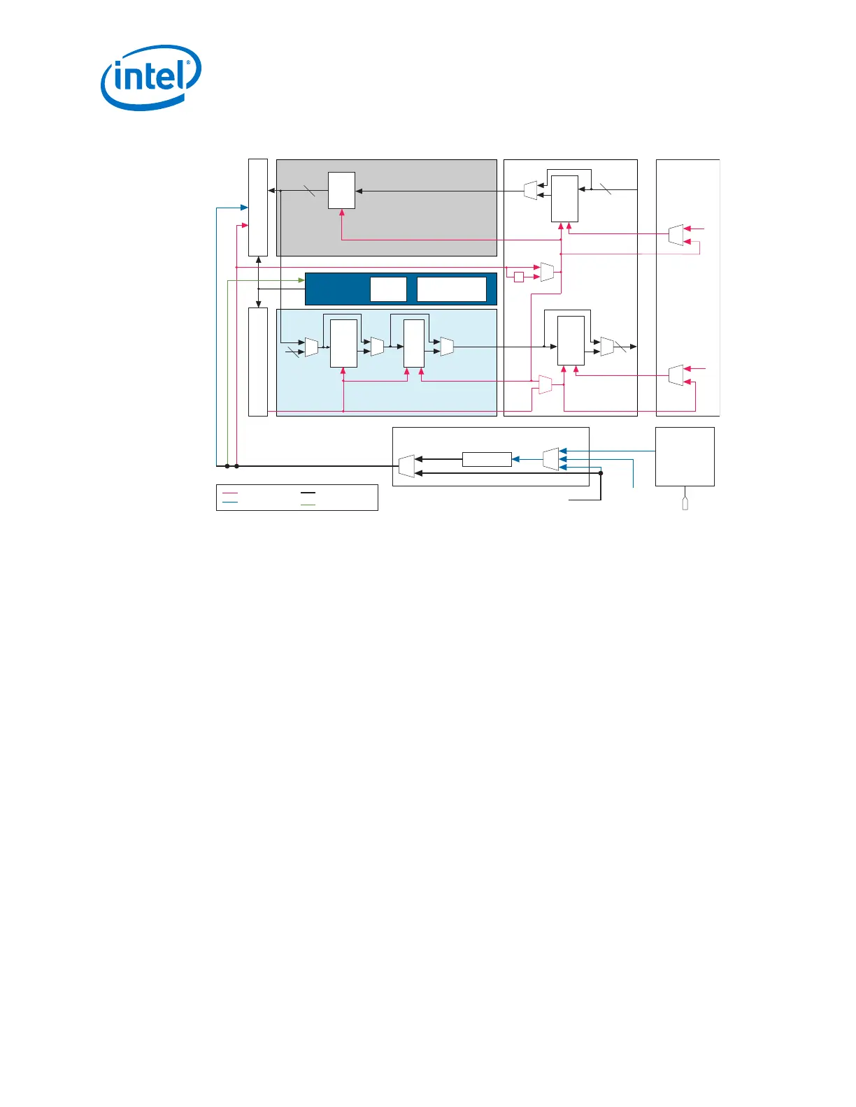
Figure 264. Gen3 PCS Block Diagram
32
32
32
32
Rate Match
FIFO
Auto-Speed Negotiation
Gen3 x1, x2, x4, x8
CDR
Control
TX
PMA
RX
PMA
PIPE Interface
TX PCIe Gen3 PCS
RX PCIe Gen3 PCS
TX Phase
Compensation
FIFO
RX Phase
Compensation
FIFO
Gearbox
/4
Standard
PCS
Block
Synchronizer
rx_clkout
pll_pcie_clk
tx_clkout
rx_coreclkin
rx_clkout or
tx_clkout
rx_clkout or
tx_clkout
FPGA
Fabric
tx_coreclkin
tx_clkout
Clock Divider
Parallel and Serial Clocks
Clock Generation Block (CGB)
Serial Clock
Input Reference Clock
ATX PLL
fPLL
tx_clkouttx_clkout
Serial Clock
Parallel and Serial Clocks
hclk for ASN Block
tx_clkout or rx_clkout
Related Information
• PCI Express (PIPE) on page 229
For more information about PCIe Gen1, Gen2, and Gen3 implementation and
configuration, refer to "Supported PIPE Features."
• Intel Arria 10 Hard IP for PCIe IP Cores
5.4.1. Transmitter Datapath
This section describes the TX FIFO and the Gearbox of the Gen3 PCS transmitter.
5.4.1.1. TX FIFO (Shared with Standard and Enhanced PCS)
The TX FIFO in each channel ensures a reliable transfer of data and status signals
between the PCS channel and the FPGA fabric. The TX FIFO compensates for the
phase difference between the low speed parallel PCS clock and the FPGA fabric clock.
The RX and TX FIFOs are shared with standard and enhanced PCS. In Hard IP mode,
the TX FIFO works in register mode. In PIPE mode, the TX FIFO works in low latency
mode.
The TX FIFO operates in low latency mode in PIPE Gen1, Gen2, and Gen3
configurations. The Low Latency mode incurs 3-4 cycles of latency when connecting
with the FPGA fabric. The FIFO empty and the FIFO full threshold values are made
closer so that the depth of the FIFO decreases, which decreases the latency.
Related Information
Arria 10 Standard PCS Architecture on page 479
For more information about TX FIFO.
5. Arria 10 Transceiver PHY Architecture
UG-01143 | 2018.06.15
Intel
®
Arria
®
10 Transceiver PHY User Guide
496