Related Information
Calibration on page 567
For more information about the calibration process
3.2.1. Dedicated Reference Clock Pins
To minimize the jitter, the advanced transmit (ATX) PLL and the fractional PLL (fPLL)
can source the input reference clock directly from the reference clock buffer without
passing through the reference clock network. The input reference clock is also fed into
the reference clock network.
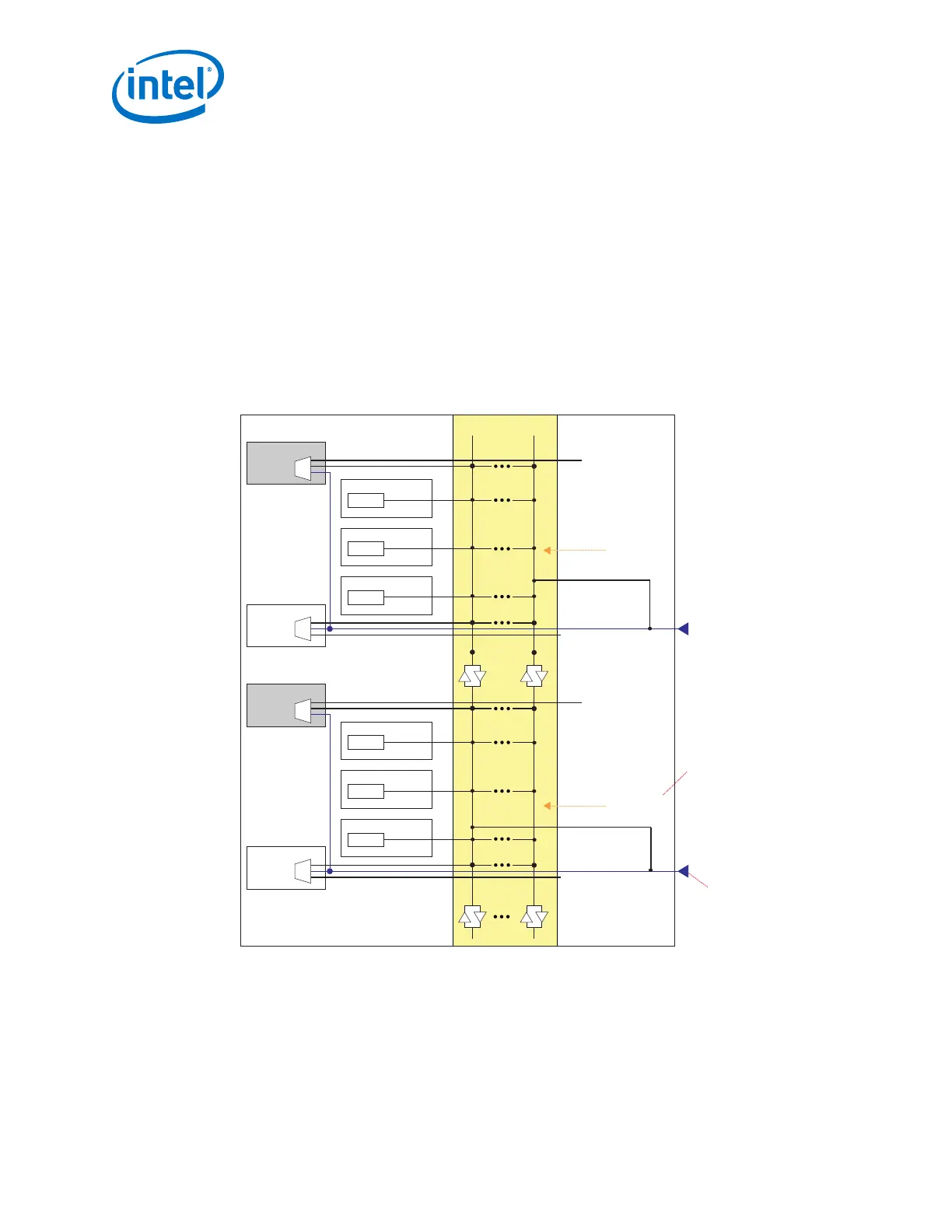
Figure 174. Dedicated Reference Clock Pins
There are two dedicated reference clock (refclk) pins available in each transceiver bank. The bottom refclk
pin feeds the bottom ATX PLL, fPLL, and CMU PLL. The top refclk pin feeds the top ATX PLL, fPLL, and CMU
PLL. The dedicated reference clock pins can also drive the reference clock network.
Refclk
CH5
CMU PLL
CH4
CDR PLL
CH3
fPLL1
ATX PLL1
CDR PLL
From PLL
Cascading Clock
Network
From PLL Feedback
and Cascading Clock
Network
Refclk
CH2
CMU PLL
CH1
CDR PLL
CH0
fPLL0
ATX PLL0
CDR PLL
Reference Clock
Network
Reference Clock
Network
Reference Clock
Network
Input Reference Clock to the PLLs
Can Come from Either the Reference
Clock Network or the PLL Feedback
and Cascading Clock Network
ATX and fPLL Can Receive the
Input Reference Clock from a
Dedicated refclk Pin
From PLL
Cascading Clock
Network
From PLL Feedback
and Cascading Clock
Network
3.2.2. Receiver Input Pins
Receiver input pins can be used as an input reference clock source to transceiver PLLs.
However, they cannot be used to drive core fabric.
3. PLLs and Clock Networks
UG-01143 | 2018.06.15
Intel
®
Arria
®
10 Transceiver PHY User Guide
374