Arria 10 transceiver PLLs have five possible input reference clock sources, depending
on jitter requirements:
• Dedicated reference clock pins
• Reference clock network
• The output of another fPLL with PLL cascading
(58)
• Receiver input pins
• Global clock or core clock
(58)
For the best jitter performance, Intel recommends placing the reference clock as close
as possible, to the transmit PLL. For protocol jitter compliance at data rates > 10
Gbps, place the reference clock pin in the same triplet as the transmit PLL.
The following protocols require the reference clock to be placed in same bank as the
transmit PLL:
• OTU2e, OTU2, OC-192 and 10G PON
• 6G and 12G SDI
Note: Sourcing a reference clock from a cascaded PLL output, global clock or core clock
network introduces additional jitter to transmit PLL output. Refer to KDB "How do I
compensate for the jitter of PLL cascading or non-dedicated clock path for Arria 10 PLL
reference clock?" for more details.
For optimum performance of GT channel, the reference clock of transmit PLL is
recommended to be from a dedicated reference clock pin in the same bank.
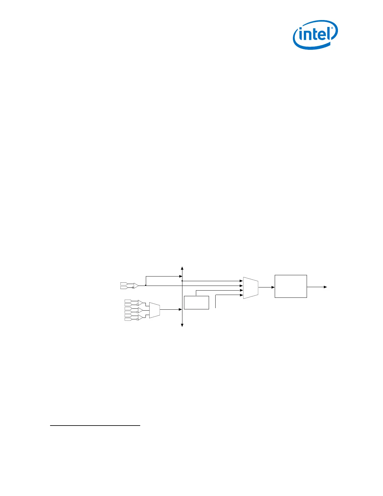
Figure 173. Input Reference Clock Sources
Dedicated
refclk
pin
RX pin 2
RX pin 1
Note : (1) You can choose only one of the three RX pins to be used as an input reference clock source. Any RX pin on the same side
of the device can be used as an input reference clock.
RX pin 0
Reference Clock
Network
Serial Clock
fPLL or ATX PLL
fPLL
Input
Reference
Clock
(2)
(3)
(2) Dedicated refclk pin can be used as an input reference clock source only for ATX or fPLL or to the reference clock network.
Reference clock network can then drive the CMU PLL.
(3) The output of another PLL can be used as an input reference clock source during PLL cascading. Arria 10 transceivers support fPLL to fPLL cascading.
(1)
Global or
Core Clock
Note: • In Arria 10 devices, the FPGA fabric core clock network can be used as an input
reference source for any PLL type.
• To successfully complete the calibration process, the reference clocks driving the
PLLs (ATX PLL, fPLL, CDR/CMU PLL) must be stable and free running at start of
FPGA configuration. Otherwise, recalibration is necessary.
(58)
Not available for CMU.
3. PLLs and Clock Networks
UG-01143 | 2018.06.15
Intel
®
Arria
®
10 Transceiver PHY User Guide
373