The output frequency of tx_pma_div_clkout and rx_pma_div_clkout can be one
of the following:
•
A divided down version of the tx_clkout or rx_clkout respectively, where
divide by 1 and divide by 2 ratios are available.
• A divided down version of the serializer clock where divide by 33, 40, and 66
ratios are available.
Note: Refer to the "TX PMA Optional Ports" table in PMA Parameters section for details about
selecting the division factor.
These clocks can be used to meet core timing by operating the TX and RX FIFO in
double-width mode, as this halves the required clock frequency at the PCS to/from
FPGA interface. These clocks can also be used to clock the core side of the TX and RX
FIFOs when the Enhanced PCS Gearbox is used.
For example, if you use the Enhanced PCS Gearbox with a 66:40 ratio, then you can
use tx_pma_div_clkout with a divide-by-33 ratio to clock the write side of the TX
FIFO, instead of using a PLL to generate the required clock frequency, or using an
external clock source.
Related Information
PMA Parameters on page 51
3.6. Transmitter Data Path Interface Clocking
The clocks generated by the PLLs are used to clock the channel PMA and PCS blocks.
The clocking architecture is different for the standard PCS and the enhanced PCS.
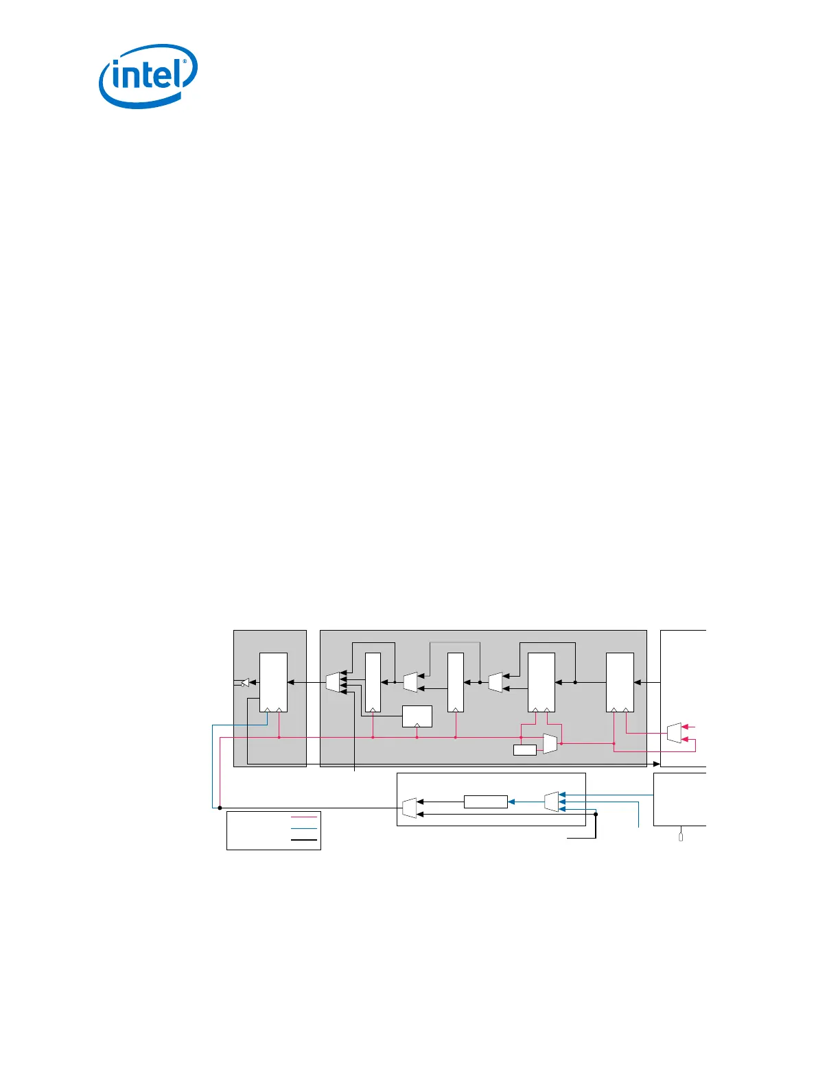
Figure 181. Transmitter Standard PCS and PMA Clocking
The master or the local CGB provides the high speed serial clock to the serializer of the transmitter PMA, and
the low speed parallel clock to the transmitter PCS.
Input Reference Clock
Transmitter Standard PCS
Transmitter PMA
Serializer
tx_serial_data
FPGA
Fabric
TX
FIFO
Byte Serializer
8B/10B Encoder
PRBS
Generator
TX Bit Slip
/2, /4
Parallel Clock
Serial Clock
Parallel and Serial Clock
Parallel and Serial Clock
Clock Divider
Serial Clock
Clock Generation Block (CGB)
ATX PLL
CMU PLL
fPLL
tx_coreclkin
tx_clkout
tx_clkout
tx_pma_div_clkout
From Receiver Standard PCS
In the Standard PCS, for configurations that do not use the byte serializer, the parallel
clock is used by all the blocks up to the read side of the TX phase compensation FIFO.
For configurations that use the byte serializer block, the clock divided by 2 or 4 is used
by the byte serializer and the read side of the TX phase compensation FIFO. The clock
used to clock the read side of the TX phase compensation FIFO is also forwarded to
the FPGA fabric to provide an interface between the FPGA fabric and the transceiver.
3. PLLs and Clock Networks
UG-01143 | 2018.06.15
Intel
®
Arria
®
10 Transceiver PHY User Guide
386