5.3.1.1.1. TX FIFO Low Latency Mode
The low latency mode incurs two to three cycles of latency (latency uncertainty) when
connecting it with the FPGA fabric. The FIFO empty and the FIFO full threshold values
are made closer so that the depth of the FIFO decreases, which in turn decreases the
latency.
5.3.1.1.2. TX FIFO Register Mode
The register mode bypasses the FIFO functionality to eliminate the FIFO latency
uncertainty for applications with stringent latency requirements. This is accomplished
by tying the read clock of the FIFO with its write clock. The register mode incurs only
one clock cycle of latency when interfacing to the FPGA fabric.
5.3.1.1.3. TX FIFO Fast Register Mode
This mode allows a higher maximum frequency (f
MAX
) between the FPGA fabric and
the TX PCS by enabling the optional fast register interface with additional latency.
5.3.1.2. Byte Serializer
In certain applications, the FPGA fabric cannot operate at the same clock rate as the
transmitter channel (PCS) because the transmitter channel is capable of operating at
higher clock rates compared to the FPGA fabric. The byte serializer allows the
transmitter channel to operate at higher data rates while keeping the FPGA fabric
interface clock rate below its maximum limit. This is accomplished by increasing the
channel width two or four times (FPGA fabric-to-PCS interface width) and dividing the
clock (tx_clkout) rate by 2 or 4. The byte serializer can be disabled, or operate in
Serialize x2 or Serialize x4 modes.
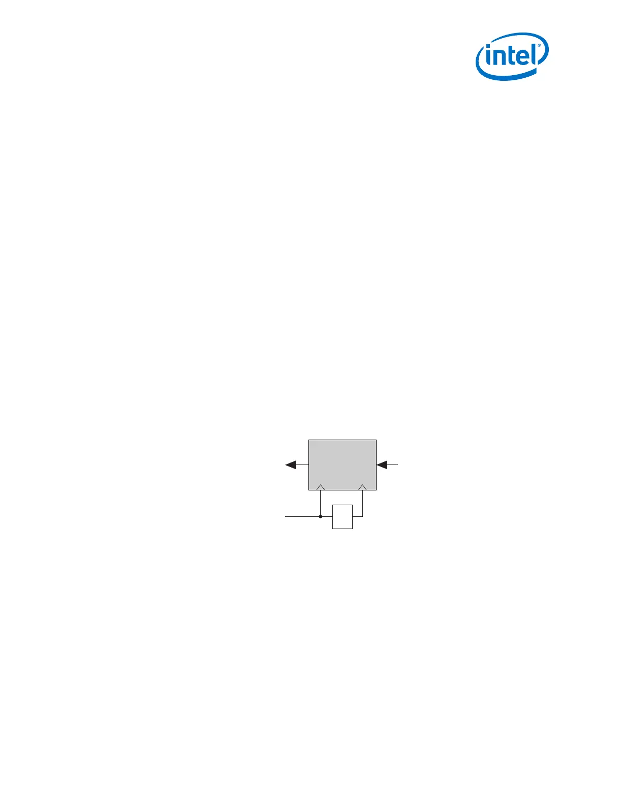
Figure 254. Byte Serializer Block Diagram
Byte
Serializer
dataout
(to the 8B/10 Encoder
or the TX Bit Slip)
datain (from the TX FIFO)
/2,
/4
tx_clkout
Related Information
• Resetting Transceiver Channels on page 416
• Implementing Protocols in Arria 10 Transceivers on page 32
5.3.1.2.1. Bonded Byte Serializer
The bonded byte serializer is available in Arria 10 devices, and is used in applications
such as PIPE, CPRI, and custom applications where multiple channels are grouped
together. The bonded byte serializer is implemented by bonding all the control signals
to prevent skew induction between channels during byte serialization. In this
configuration, one of the channels acts as master and the remaining channels act as
slaves.
5. Arria 10 Transceiver PHY Architecture
UG-01143 | 2018.06.15
Intel
®
Arria
®
10 Transceiver PHY User Guide
481