Port Direction Clock Domain Description
pcie_sw[1:0] Input Asynchronous 2-bit rate switch control input used for
PCIe protocol implementation.
pcie_sw_done[1:0] Output Asynchronous 2-bit rate switch status output used for
PCIe protocol implementation.
atx_to_fpll_cascade_clk Output N/A The ATX PLL output clock is used to
drive fPLL reference clock input (only
available in SDI_cascade or
OTN_cascade protocol mode).
ext_lock_detect_clklow
(55)
Output N/A
Clklow output for external lock
detection. It can be exposed by
selecting the Enable clklow and fref
port
ext_lock_detect_fref
(55)
Output N/A Fref output for external lock detection.
It can be exposed by selecting the
Enable clklow and fref port.
Related Information
• Calibration on page 29
• Avalon Interface Specifications
The ports related to reconfiguration are compliant with the Avalon specification.
Refer to the Avalon specification for more details about these ports.
• Intel Arria 10 Device Datasheet
Refer to the Intel Arria 10 Device Datasheet for more details about the PLL
output frequency range.
• Reconfiguration Interface and Dynamic Reconfiguration on page 502
• Reconfiguring Channel and PLL Blocks on page 503
• Steps to Perform Dynamic Reconfiguration on page 516
• Intel Arria 10 device fPLL reports an unlocked condition
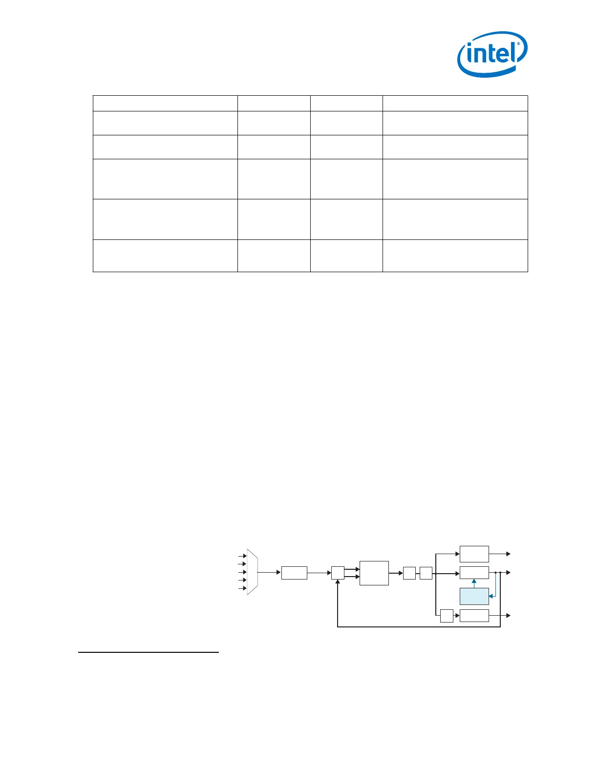
3.1.3. fPLL
There are two fPLLs in each transceiver bank with six channels (one located at the top
and the other at the bottom of the bank). Transceiver banks with three channels have
only one fPLL.
Figure 171. fPLL Block Diagram
VCO
PFD
Up
Down
Delta Sigma
Modulator
L Counter
/1, 2, 4, 8
N Counter
M Counter
Charge
Pump and
Loop Filter
C Counter
Refclk
Multiplexer
Reference Clock Network
Receiver Input Pin
Output of Another PLL with PLL Cascading
Dedicated Reference Clock Pin
Global Clock or Core Clock
refclk
Input
Reference
Clock
fbclk
/2
/2
(55)
The fPLL fref and clklow signals should only be used with the Intel external soft lock
detection logic.
3. PLLs and Clock Networks
UG-01143 | 2018.06.15
Intel
®
Arria
®
10 Transceiver PHY User Guide
359