Figure 252. Standard PCS Datapath Diagram
RX
FIFO
Byte
Deserializer
8B/10B Decoder
Rate Match FIFO
Receiver PMA
Word Aligner
Deserializer
CDR
Receiver Standard PCS
Transmitter Standard PCS
Transmitter PMA
Serializer
tx_serial_data
rx_serial_data
FPGA
Fabric
TX
FIFO
Byte Serializer
8B/10B Encoder
PRBS
Generator
TX Bit Slip
/2, /4
/2, /4
Parallel Clock
Serial Clock
Parallel and Serial Clock
Parallel and Serial Clock
Clock Divider
rx_pma_div_clkout
Serial Clock
Clock Generation Block (CGB)
ATX PLL
CMU PLL
fPLL
tx_coreclkin
rx_coreclkin
rx_clkout or
tx_clkout
Parallel Clock
(Recovered)
Parallel Clock
(From Clock
Divider)
tx_clkout
tx_clkout
tx_clkout
rx_clkout
PRBS
Verifier
tx_pma_div_clkout
5.3.1. Transmitter Datapath
5.3.1.1. TX FIFO (Shared with Enhanced PCS and PCIe Gen3 PCS)
The TX FIFO interfaces between the transmitter PCS and the FPGA fabric and ensures
reliable transfer of data and status signals. It compensates for the phase difference
between the FPGA fabric clock and tx_clkout (the low-speed parallel clock). The TX
FIFO has a depth of 8 and operates in low latency mode, register mode, and fast
register mode.
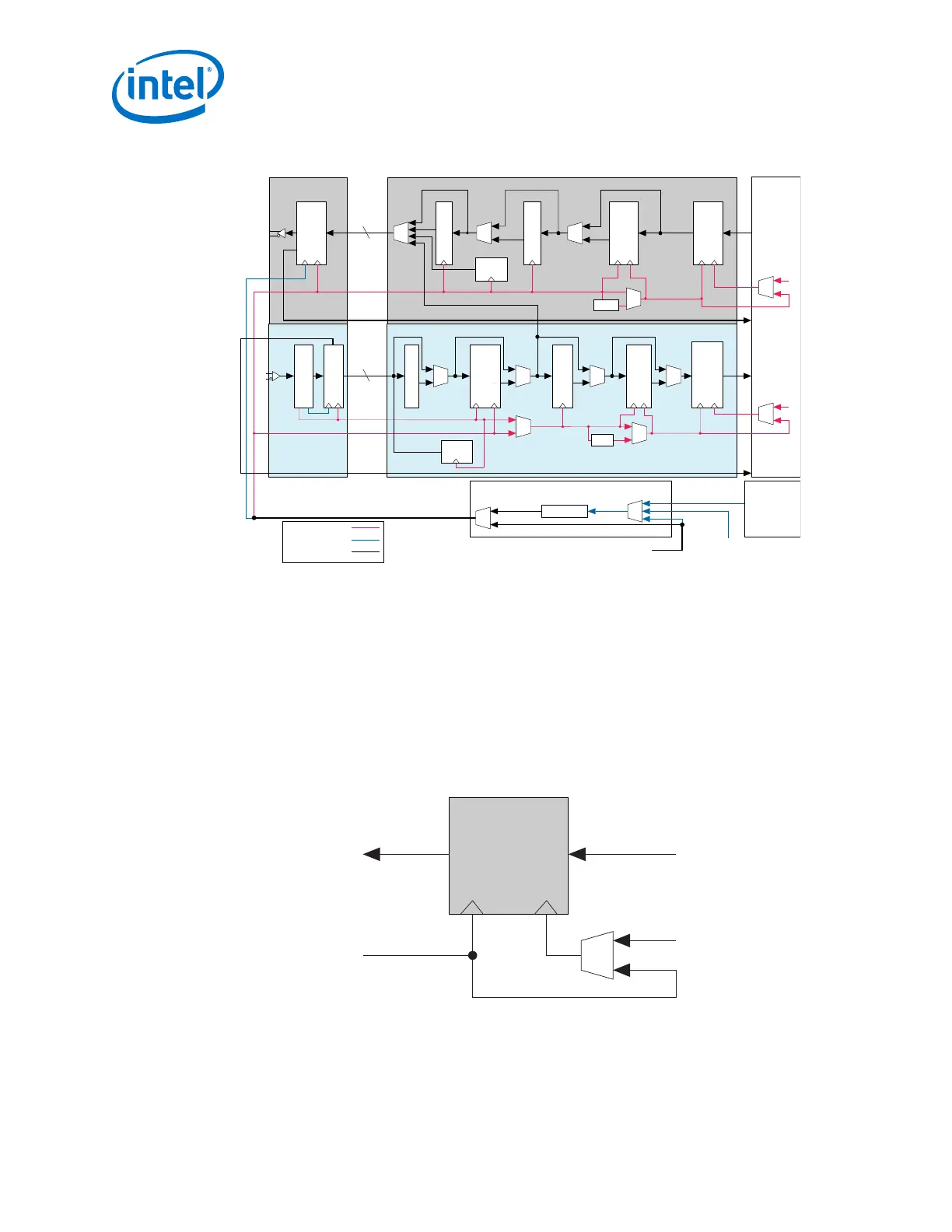
Figure 253. TX FIFO Block Diagram
TX
FIFO
Datapath from FPGA Fabric
or PIPE Interface
tx_coreclkin
tx_clkout
Datapath to Byte Serializer,
8B/10B Encoder,
or Serializer
wr_clkrd_clk
You can control the write port using tx_clkout or tx_coreclkin. Use the
tx_clkout signal for a single channel and tx_coreclkin when using multiple
channels. The TX FIFO is shared with PCIe Gen3 and Enhanced PCS data paths.
5. Arria 10 Transceiver PHY Architecture
UG-01143 | 2018.06.15
Intel
®
Arria
®
10 Transceiver PHY User Guide
480