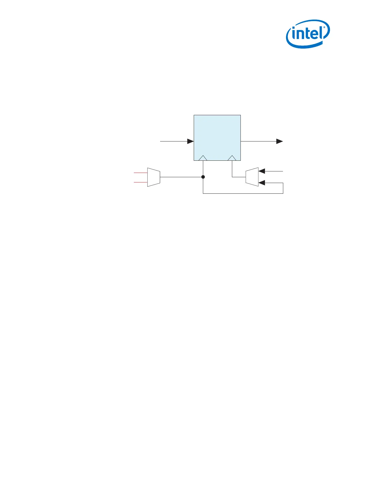
5.3.2.7. RX FIFO (Shared with Enhanced PCS and PCIe Gen3 PCS)
The RX FIFO interfaces between the PCS on the receiver side and the FPGA fabric and
ensures reliable transfer of data and status signals. It compensates for the phase
difference between the FPGA fabric and the PCS on the receiver side. The RX FIFO has
a depth of 8. It operates in register FIFO and low latency modes.
Figure 263. RX FIFO Block Diagram
RX
FIFO
Datapath to FPGA Fabric
or PIPE Interface
rx_coreclkin
Datapath from
Byte Deserializer, 8B/10B Decoder,
Rate Match FIFO, or Deserializer
wr_clk rd_clk
Parallel clock
(recovered)
from clock divider
rx_clkout
5.3.2.7.1. RX FIFO Low Latency Mode
The low latency mode incurs two to three cycles of latency when connecting it with the
FPGA fabric. The FIFO empty and the FIFO full threshold values are made closer so
that the depth of the FIFO decreases, which in turn decreases the latency.
5.3.2.7.2. RX FIFO Register Mode
The register mode bypasses the FIFO functionality to eliminate the FIFO latency
uncertainty for applications with stringent latency requirements. This is accomplished
by tying the read clock of the FIFO with its write clock. The register mode incurs only
one clock cycle of latency when interfacing to the FPGA fabric.
5.4. Arria 10 PCI Express Gen3 PCS Architecture
Arria 10 architecture supports the PCIe Gen3 specification. Intel provides two options
to implement the PCI Express solution:
• You can use the Intel Hard IP solution. This complete package provides both the
MAC layer and the physical (PHY) layer functionality.
• You can implement the MAC in the FPGA core and connect this MAC to the
transceiver PHY through the PIPE interface.
This section focuses on the basic blocks of PIPE 3.0-based Gen3 PCS architecture. The
PIPE 3.0-based Gen3 PCS uses a 128b/130b block encoding/decoding scheme, which
is different from the 8B/10B scheme used in Gen1 and Gen2. The 130-bit block
contains a 2-bit sync header and a 128-bit data payload. For this reason, Arria 10
devices include a separate Gen3 PCS that supports functionality at Gen3 speeds. This
PIPE interface supports the seamless switching of Data and Clock between the Gen1,
Gen2, and Gen3 data rates, and provides support for PIPE 3.0 features. The PCIe
Gen3 PCS supports the PIPE interface with the Hard IP enabled, as well as with the
Hard IP bypassed.
5. Arria 10 Transceiver PHY Architecture
UG-01143 | 2018.06.15
Intel
®
Arria
®
10 Transceiver PHY User Guide
495