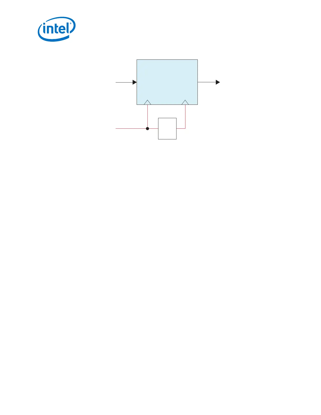
Figure 262. Byte Deserializer Block Diagram
Byte
Deserializer
Datapath from the
8B/10B Decoder,
Rate Match FIFO,
or Word Aligner
Datapath to the RX PCS FIFO
/2,
/4
Low speed
parallel clock
5.3.2.6.1. Byte Deserializer Disabled Mode
In disabled mode, the byte deserializer is bypassed. The data from the 8B/10B
decoder, rate match FIFO, or word aligner is directly transmitted to the RX FIFO,
depending on whether or not the 8B/10B decoder and rate match FIFO are enabled.
Disabled mode is used in low speed applications such as GigE, where the FPGA fabric
and the PCS can operate at the same clock rate.
5.3.2.6.2. Byte Deserializer Deserialize x2 Mode
The deserialize x2 mode is used in high-speed applications such as the PCIe Gen1 or
Gen2 protocol implementation, where the FPGA fabric cannot operate as fast as the TX
PCS.
In deserialize x2 mode, the byte deserializer deserializes 8-bit, 10-bit (when the
8B/10B encoder is not enabled), 16-bit, and 20-bit (when the 8B/10B encoder is not
enabled) input data into 16-bit, 20-bit, 32-bit, and 40-bit data, respectively. As the
parallel data width from the word aligner is doubled, the clock rate is halved.
5.3.2.6.3. Byte Deserializer Deserialize x4 Mode
The deserialize x4 mode is used in high-speed applications where the FPGA fabric
cannot operate as fast as the TX PCS.
In deserialize x4 mode, the byte deserializer deserializes 8-bit data into 32-bit data.
As the parallel data width from the word aligner is quadrupled, the clock rate is
divided four times.
5.3.2.6.4. Bonded Byte Deserializer
The bonded byte deserializer is also available for channel-bundled applications such as
PIPE. In this configuration, the control signals of the byte deserializers of all the
channels are bonded together. A master channel controls all the other channels to
prevent skew between the channels.
5. Arria 10 Transceiver PHY Architecture
UG-01143 | 2018.06.15
Intel
®
Arria
®
10 Transceiver PHY User Guide
494