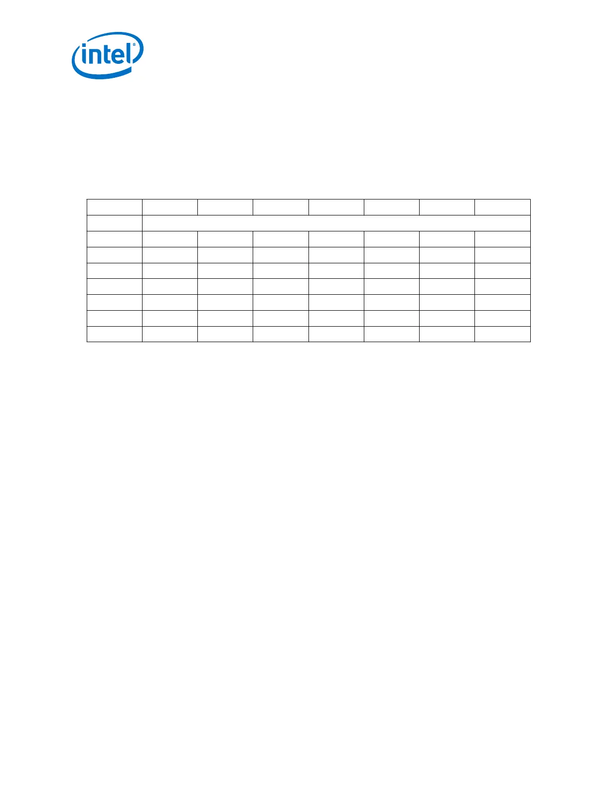
Table 5. Package Details for SX Devices with Transceivers and Hard IP Blocks Located
on the Left Side Periphery of the Device
• Package U19: 19mm x 19mm package; 484 pins.
• Package F27: 27mm x 27mm package; 672 pins.
• Package F29: 29mm x 29mm package; 780 pins.
• Packages F34 and F35: 35 mm x 35 mm package size; 1152 pins.
• Package F40: 40 mm x 40 mm package size; 1517 pins. K = 36 transceiver channels, N = 48 transceiver
channels.
Device U19 F27 F29 F34 F35 K F40 N F40
Transceiver Count, PCIe Hard IP Block Count
SX 016 6, 1 12, 1 12, 1
SX 022 6, 1 12, 1 12, 1
SX 027 12, 1 12, 1 24, 2 24, 2
SX 032 12, 1 12, 1 24, 2 24, 2
SX 048 12, 1 24, 2 36, 2
SX 057 24, 2 36, 2 36, 2 48, 2
SX 066 24, 2 36, 2 36, 2 48, 2
1.2. Transceiver PHY Architecture Overview
A link is defined as a single entity communication port. A link can have one or more
transceiver channels. A transceiver channel is synonymous with a transceiver lane.
For example, a 10GBASE-R link has one transceiver channel or lane with a data rate of
10.3125 Gbps. A 40GBASE-R link has four transceiver channels. Each transceiver
channel operates at a lane data rate of 10.3125 Gbps. Four transceiver channels give
a total collective link bandwidth of 41.25 Gbps (40 Gbps before and after 64B/66B
Physical Coding Sublayer (PCS) encoding and decoding).
1.2.1. Transceiver Bank Architecture
The transceiver bank is the fundamental unit that contains all the functional blocks
related to the device's high speed serial transceivers.
Each transceiver bank includes six transceiver channels in all devices except for the
devices with 66 transceiver channels. Devices with 66 transceiver channels have both
six channel and three channel transceiver banks. The uppermost transceiver bank on
the left and the right side of these devices is a three channel transceiver bank. All
other devices contain only six channel transceiver banks.
The figures below show the transceiver bank architecture with the phase locked loop
(PLL) and clock generation block (CGB) resources available in each bank.
1. Arria
®
10 Transceiver PHY Overview
UG-01143 | 2018.06.15
Intel
®
Arria
®
10 Transceiver PHY User Guide
20