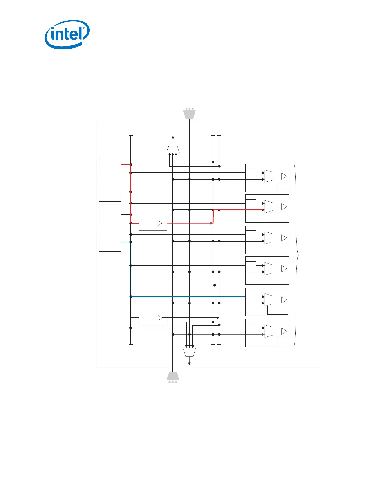
Figure 179. Clock Generation Block and Clock Network
The local clock for each transceiver channel can be sourced from either the local CGB via the x1 network, or
the master CGB via the x6/xN network. For example, as shown by the red highlighted path, the fPLL 1 drives
the x1 network which in turn drives the master CGB. The master CGB then drives the x6 clock network which
routes the clocks to the local channels. As shown by the blue highlighted path, the ATX PLL 0 can also drive the
x1 clock network which can directly feed a channel's local CGB. In this case, the low speed parallel clock is
generated by the local CGB.
CMU or CDR
CGB
Ch 4
CDR
CGB
Ch 3
CDR
CGB
Ch 2
CMU or CDR
CGB
Ch 1
CDR
CGB
Ch 0
CDR
CGB
Ch 5
Master
CGB1
Master
CGB0
xN
Up
x1
Network
ATX PLL 1
fPLL 1
fPLL 0
ATX PLL 0
Transceiver
Bank
xN
Down
x6
Top
x6
Bottom
3.5. FPGA Fabric-Transceiver Interface Clocking
The FPGA fabric-transceiver interface consists of clock signals from the FPGA fabric
into the transceiver and clock signals from the transceiver into the FPGA fabric. These
clock signals use the global (GCLK), regional (RCLK), and periphery (PCLK) clock
3. PLLs and Clock Networks
UG-01143 | 2018.06.15
Intel
®
Arria
®
10 Transceiver PHY User Guide
384