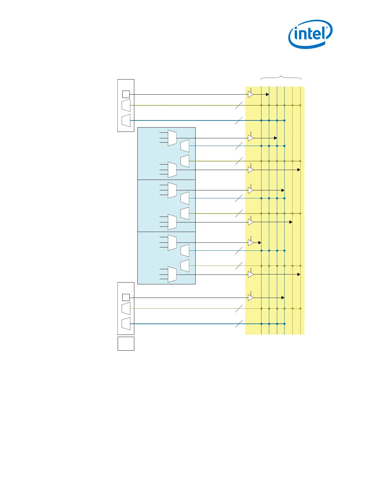
Figure 189. Integer Mode phase aligned and external feedback
pm_iqtxrx_t[5:0]
0 1 2 3 4 5
Ch5
4
6
fbclk
refclk
PMA_RX_CLK
PMA_TX_CLK
RX pin (1)
RX pin (1)
RX pin (1)
RX pin (1)
RX pin (1)
RX pin (1)
PMA_RX_CLK
PMA_TX_CLK
ch5_iqtxrxclk_2
pm_iqtxrxclk_top[5:0]
pm_iqtxrxclk_top[3:0]
ch5_iqtxrxclk_5
Ch4
4
6
fbclk
refclk
PMA_RX_CLK
PMA_TX_CLK
PMA_RX_CLK
PMA_TX_CLK
ch4_iqtxrxclk_4
pm_iqtxrxclk_top[5:0]
pm_iqtxrxclk_top[3:0]
ch4_iqtxrxclk_4
Ch3
4
6
fbclk
refclk
PMA_RX_CLK
PMA_TX_CLK
PMA_RX_CLK
PMA_TX_CLK
ch3_iqtxrxclk_0
pm_iqtxrxclk_top[5:0]
pm_iqtxrxclk_top[3:0]
ch3_iqtxrxclk_5
fPLL 1
6
4
refclk
fbclk
fpll_t_iqtxrxclk
pm_iqtxrxclk_top[5:0]
pm_iqtxrxclk_top[3:0]
C
LCPLL 1
6
4
refclk
fbclk
lc_t_iqtxrxclk
pm_iqtxrxclk_top[5:0]
pm_iqtxrxclk_top[3:0]
M
Master
CGB 1
Note: (1) RX pin used as reference clock
You must recalibrate the fPLL when you enable the phase alignment option.
1. Modify the fPLL IP to enable fPLL reconfiguration
• Under the Dynamic Reconfiguration Tab, turn ON Enable dynamic
reconfiguration.
2. Create logics in the core to perform following steps:
3. PLLs and Clock Networks
UG-01143 | 2018.06.15
Intel
®
Arria
®
10 Transceiver PHY User Guide
397